Pre-cleaning chambers and semiconductor processing equipment

A pre-cleaning and chamber technology, applied in semiconductor/solid-state device manufacturing, discharge tubes, electrical components, etc., can solve problems such as uneven gas distribution, different path lengths, process gas waste, etc., to improve the uniformity of gas distribution , Shorten time and reduce waste

Active Publication Date: 2019-01-18
BEIJING NAURA MICROELECTRONICS EQUIP CO LTD
View PDF3 Cites 0 Cited by
  • Summary
  • Abstract
  • Description
  • Claims
  • Application Information

AI Technical Summary

Problems solved by technology

[0006] First, the path for the process gas to enter the process chamber is too long, so it takes a long time to reach the process chamber, which affects the process efficiency
[0007] Second, because the air pressure in the process chamber is greater than the air pressure near the vacuum pump port, and the vacuum pump is always in working condition during the process, most of the process gas is directly sucked away by the vacuum pump before entering the process chamber, so it needs to pass The intake pipeline continuously replenishes a large amount of process gas to maintain the plasma in an excited state, and more process gas is required to achieve the required plasma density, resulting in waste of process gas
[0008] Third, since there is only one inlet pipeline, it transports the process gas to the loading and unloading chamber from a single direction, which makes the path length of the process gas to the process chamber different, resulting in uneven gas distribution

Method used


Image

  • Pre-cleaning chambers and semiconductor processing equipment
  • Pre-cleaning chambers and semiconductor processing equipment
  • Pre-cleaning chambers and semiconductor processing equipment

Examples


Embodiment Construction

[0026] In order for those skilled in the art to better understand the technical solutions of the present invention, the pre-cleaning chamber and semiconductor processing equipment provided by the present invention will be described in detail below in conjunction with the accompanying drawings.

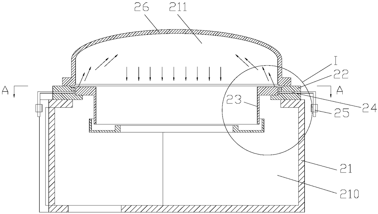
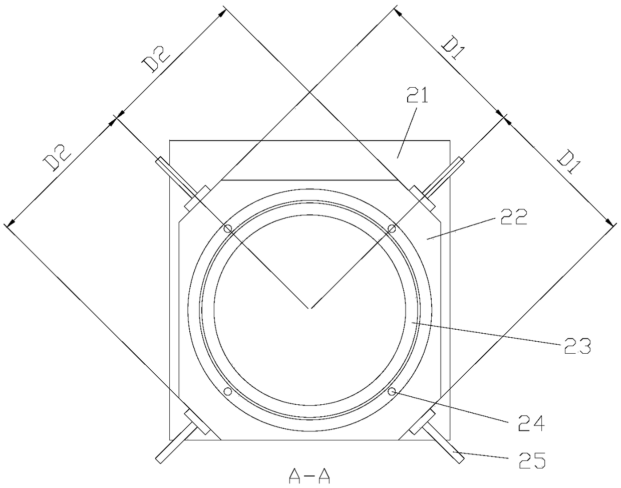
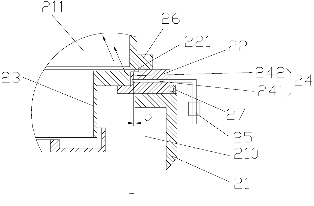
[0027] figure 1 A cross-sectional view of a pre-cleaning chamber provided for an embodiment of the present invention. figure 2 for figure 1 A top view along the line A-A. image 3 for figure 1 Zoom-in view of the middle I region. Please also refer to Figure 1-3 , the pre-cleaning chamber is formed by a chamber body 21 and a medium window 26 arranged on the top of the chamber body 21 . The dielectric window 26 is an arched top cover made of insulating material (such as ceramic or quartz). Moreover, a process component 23 is arranged around the pre-cleaning chamber, and the structure of the process component 23 is as follows: figure 1 As shown, it is a ring structure, and the sp...


PUM


Abstract

The invention provides a precleaning cavity and semiconductor processing equipment, and the precleaning cavity comprises a cavity, a dielectric window disposed at the top of the cavity, and an air incoming device. The interior of the precleaning cavity is provided with a technological module in a winding manner. A space which is limited by the technological module and the dielectric window jointly serves as a technological sub-cavity. A space, located below the technological module, of the cavity serves as a loading and unloading sub-cavity. The air incoming device comprises a plurality of gas channels which are centrosymmetric relative to the axis of the technological module, and each gas channel is communicated with the technological sub-cavity, and is used for conveying technological gas to the technological sub-cavity directly above the technological module. The precleaning cavity can shorten the air incoming path of the technological gas, reduces the waste of technological gas, also can achieve the uniform incoming of gas, and can improve the technological quality.

Description

technical field [0001] The invention relates to the field of semiconductor equipment manufacturing, and relates to a pre-cleaning chamber and semiconductor processing equipment. Background technique [0002] Plasma processing equipment is widely used in today's semiconductor integrated circuits, solar cells, flat panel displays and other manufacturing processes. Plasma processing equipment that has been widely used in the industry is of the following types: for example, a DC discharge type, a capacitive coupling (CCP) type, an inductive coupling (ICP) type, and an electron cyclotron resonance (ECR) type. These types of plasma processing equipment are currently used in processes such as deposition, etching, and cleaning. [0003] During the process, in order to improve the quality of the product, before implementing the deposition process, the wafer should be pre-cleaned (Preclean) to remove impurities such as oxides on the wafer surface. The basic principle of a general pr...

Claims


Application Information

Patent Timeline
Patent Type & Authority Patents(China)
IPC IPC(8): H01J37/32H01L21/67
CPCH01J37/3244H01L21/67023
Inventor 余志龙郑金果郭浩陈鹏赵梦欣丁培军
Owner BEIJING NAURA MICROELECTRONICS EQUIP CO LTD
Why Eureka
Try Eureka