Transparent conductive film, transparent conductive film laminate, and touch panel

A technology of transparent conductive film and transparent conductive film, applied in the direction of conductive layer, non-metallic conductor, oxide conductor, etc.

Active Publication Date: 2019-09-06
NITTO DENKO CORP
View PDF5 Cites 0 Cited by
  • Summary
  • Abstract
  • Description
  • Claims
  • Application Information

AI Technical Summary

Problems solved by technology

In this case, since the glass substrate is thin, it is easily affected by heating, and since the heat shrinkage rate and the like are different between resin and glass, the laminated body is curled, and it can...

Method used


Image

  • Transparent conductive film, transparent conductive film laminate, and touch panel
  • Transparent conductive film, transparent conductive film laminate, and touch panel
  • Transparent conductive film, transparent conductive film laminate, and touch panel

Examples


Embodiment 1

[0104] (Preparation of Curable Resin Composition Adding Spherical Particles)

[0105] Acrylic spherical particles (products manufactured by Soken Chemical Co., Ltd.) containing 100 parts by weight of an ultraviolet curable resin composition (product name "UNIDIC (registered trademark) RS29-120" manufactured by DIC Corporation) and a mode particle diameter of 1.9 μm were prepared. Name "MX-180TA") 0.3 parts by weight of curable resin composition added spherical particles.

[0106] (Formation of cured resin layer)

[0107] The prepared curable resin composition containing spherical particles was coated on one side of a polycycloolefin film (trade name "ZEONOR (registered trademark)" manufactured by ZEON Japan) with a thickness of 35 μm and a glass transition temperature of 165°C to form coating layer. Then, the coating layer was irradiated with ultraviolet rays from the side where the coating layer was formed to form a second cured resin layer so as to have a thickness of 1.0 ...

Embodiment 2

[0115] Except in Example 1, a polycycloolefin film (trade name "ZEONOR (registered trademark)" manufactured by ZEON Japan) with a thickness of 50 μm was used as the transparent resin film, and spherical particles contained in the second cured resin layer were used. A transparent conductive film and a transparent conductive film laminate were produced by the same method as in Example 1, except that particles having a mode diameter of 0.8 μm were used and the thickness of the second cured resin layer was 0.5 μm.

Embodiment 3

[0117] In Example 1, the transparent conductive film and the transparent conductive film were formed in the same manner as in Example 1, except that after the optical adjustment layer was formed, the roll-to-roll method was annealed at 150° C. for 3 minutes to form a transparent conductive film. Sexual film laminate.


PUM

PropertyMeasurementUnit
Thicknessaaaaaaaaaa
Thicknessaaaaaaaaaa
Glass transition temperatureaaaaaaaaaa

Abstract

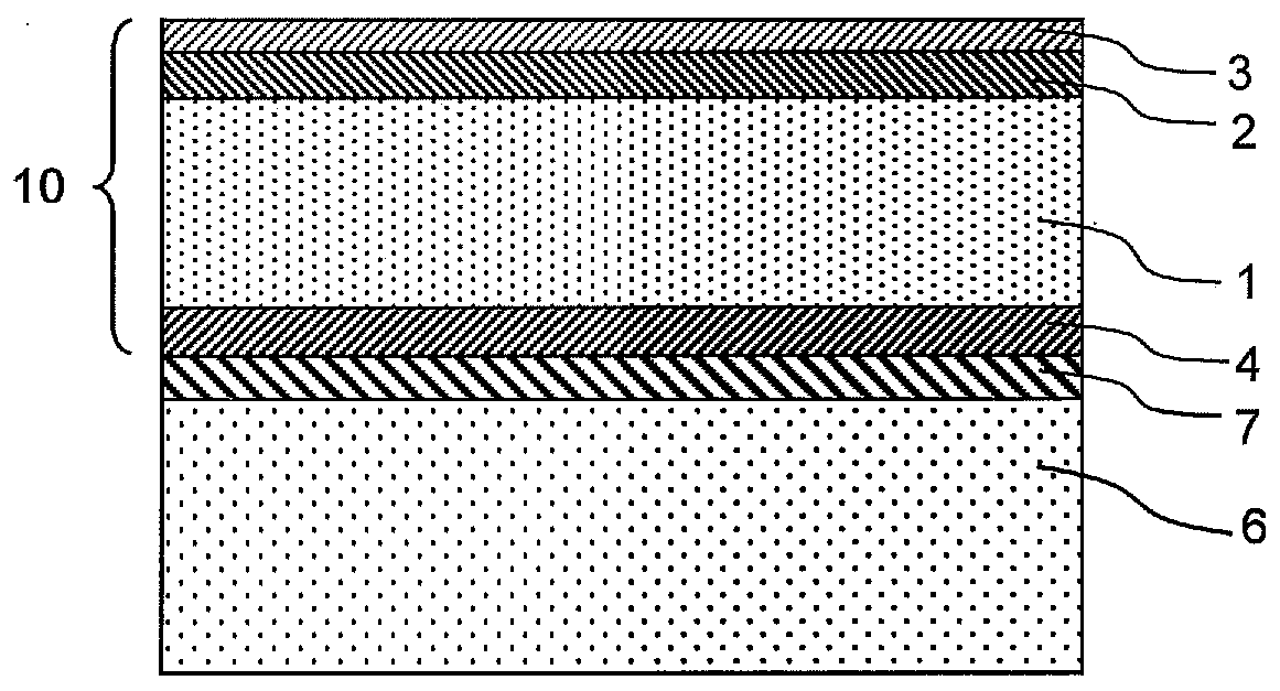
The present invention provides a transparent conductive film capable of suppressing the occurrence of curl even after a heating process in a transparent conductive film laminate in which a thin glass substrate is bonded to the transparent conductive film, and ensuring a finished product in the subsequent process. rate, and provide transparent conductive film laminates and touch panels. In the transparent conductive film (10) of the present invention, the first cured resin layer (2) and the transparent conductive film (3) are sequentially formed on one side of the transparent resin film (1), and on the other side of the transparent resin film (1) A transparent conductive film (10) with a second cured resin layer (4) is formed on the side, the transparent resin film (1) of the transparent conductive film (10) includes an amorphous resin, and the transparent conductive film (10) Cut into 50cm x 50cm, make transparent conductive film (3) as the bottom surface, and heat at 130°C for 90 minutes. The difference between the average curl value A of the four corners and the curl value B of the center, that is, A-B, is 5 mm or more .

Description

technical field [0001] The present invention relates to a transparent conductive film, a transparent conductive film laminate, and a touch panel, and is a technique that is particularly useful for controlling the occurrence of curl. Background technique [0002] Conventionally, as substrates of liquid crystal displays, organic electroluminescent displays, touch panels, and the like, members using glass as a substrate are often used. In recent years, along with the reduction in thickness of displays, reduction in thickness of glass substrates excellent in transparency, surface smoothness, heat resistance, etc. has attracted attention. [0003] On the other hand, polyethylene terephthalate (PET) is widely used as a base film of a transparent conductive film in a capacitive touch panel configuration. However, since the PET film is stretched and formed into a film, it has a high retardation, so it is difficult to use it as a polarizing plate. Therefore, in Patent Document 1, a...

Claims


Application Information

Patent Timeline
IPC IPC(8): B32B27/00G06F3/041G06F3/044
CPCB32B27/00G06F3/041G06F3/044B32B7/12B32B17/10B32B27/18B32B27/32H01B1/08H01B5/14B32B2307/412B32B2307/418B32B2307/202B32B7/023
Inventor 津野直树拜师基希细川和人
Owner NITTO DENKO CORP
Why Eureka
Try Eureka