
Transverse electric-pass polarizer based on composite waveguide
A transverse electric field and composite waveguide technology, applied in the field of optoelectronics, can solve problems such as the influence of extinction ratio, and achieve the effects of small size, reduced coupling loss, and easy optical integration
Patent Information
- Authority / Receiving Office
- CN · China
- Patent Type
- Applications(China)
- Current Assignee / Owner
- Publication Date
- 2017-09-05
- Estimated Expiration
- Not applicable · inactive patent
Smart Images
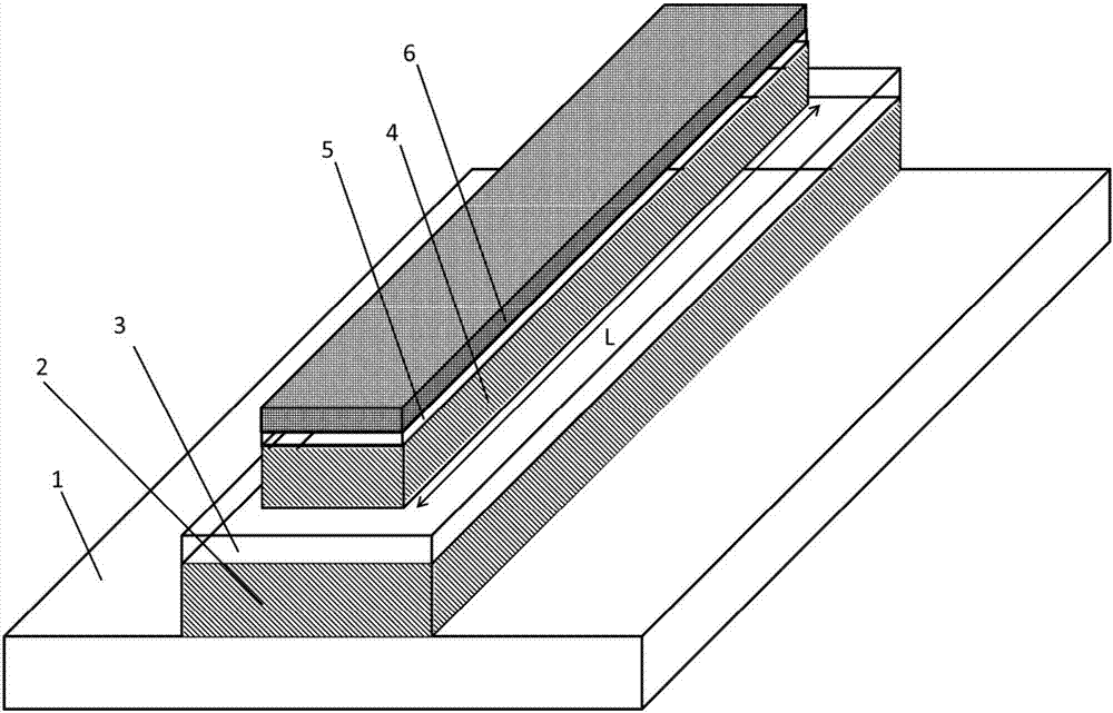
Figure 1 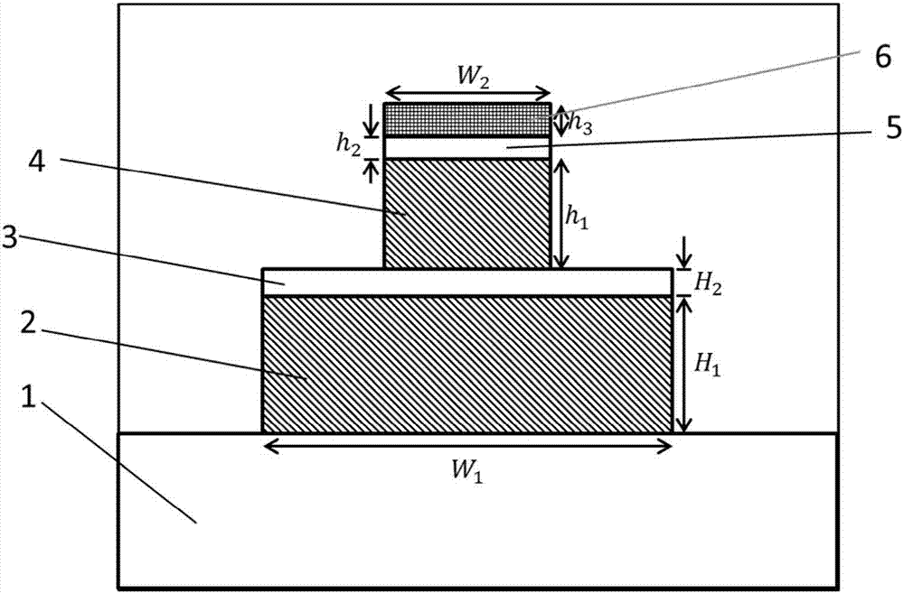
Figure 2 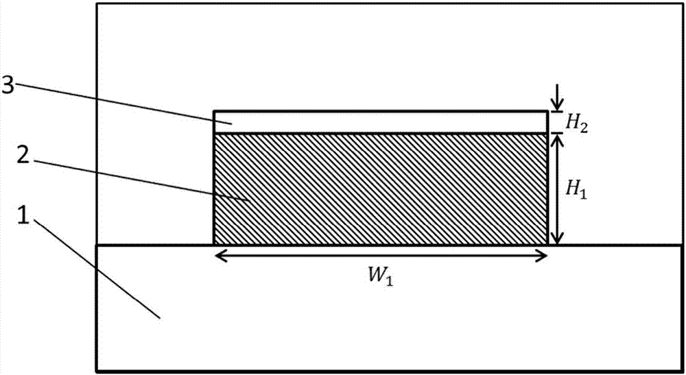
Figure 3
Abstract
Description
technical field
[0001] The invention relates to the technical field of optoelectronics, in particular to a polarizer based on a composite waveguide through which a transverse electric field passes. Background technique
[0002] With the introduction of long-distance all-optical networks, optical communication systems are becoming more and more complex. The high sensitivity of silicon-based components to the polarization of incident light has attracted people to design efficient and compact polarization control components, including polarizers, polarization beam splitters, and polarization rotators. In these polarization-controlling components, polarizers can be used to suppress the passage of unwanted polarization states and thus play an integral part in solving the polarization-dependent problems of many optical systems.
[0003] For on-chip applications, polarizers must achieve ultra-small packages, high extinction ratios, and low losses. Many TE-pass and transverse magn...
Examples
Embodiment Construction
[0033] The present invention will be described in detail below with reference to the drawings and specific embodiments.
[0034] Such as figure 1 and 2, the specific implementation of the present invention refers to as figure 1 , the three-dimensional schematic diagram of the TE-pass polarizer of this embodiment, including the incident silicon waveguide and the outgoing silicon waveguide and the intermediate coupling part between the incident silicon waveguide and the outgoing silicon waveguide.
[0035] As shown in Figure 2(a), the middle coupling part is a five-layer waveguide structure placed on the SOI substrate 1. The five-layer waveguide structure is the lower silicon layer 2, the lower silicon dioxide layer 3, and the upper silicon layer from bottom to top. 4. Upper silicon dioxide layer 5 and metallic chromium layer 6 . The upper silicon layer 4, the upper silicon dioxide layer 5 and the metal chromium layer 6 have the same width, and the length of the middle coupl...