Hafnium oxide based ferroelectric grid structure and preparation technology thereof

A preparation process, the technology of hafnium oxide, applied in the field of memory, can solve the problems of small storage window, silicon process incompatibility, interface effect, etc., and achieve the effect of vertical dimension reduction, excellent electrical performance and excellent ferroelectric performance

Active Publication Date: 2017-09-05
XIANGTAN UNIV
View PDF3 Cites 15 Cited by
  • Summary
  • Abstract
  • Description
  • Claims
  • Application Information

AI Technical Summary

Problems solved by technology

[0005] First, due to the mutual reaction and mutual diffusion between the ferroelectric film and the silicon substrate, it is difficult to form a good interface state between the ferroelectric film and the silicon substrate. The usual solution is to introduce A buffer layer is used to improve the interface performance, but the buffer layer currently studied has a huge difference in dielectric constant and thickness from the ferroelectric layer, and the partial voltage is large during the signal erasing and writing process, resulting in a lower operating voltage of the ferroelectric layer. It cannot be completely flipped, and the storage window is small, which means that a larger voltage needs to be applied to completely flip the ferroelectric layer, increasing the operating voltage
[0006] Second, most of the traditional ferroelectric materials currently used in memory, such as SBT, PZT, BTO, etc., still have many problems in the semiconductor process, such as incompatibility with silicon processes, lead pollution caused by PZT films, small energy bands and A relatively large physical thickness (usually hundreds of nanometers) is required to obtain a large remanent polarization value, which hinders the development of miniaturization of memory devices
[0007] Thirdly, the MFIS structure ferroelectric field effect transistor is currently a research hotspot because of its simple structure and high storage density. Interface effect, making storage performance worse

Method used


Image

  • Hafnium oxide based ferroelectric grid structure and preparation technology thereof
  • Hafnium oxide based ferroelectric grid structure and preparation technology thereof

Examples


Embodiment 1

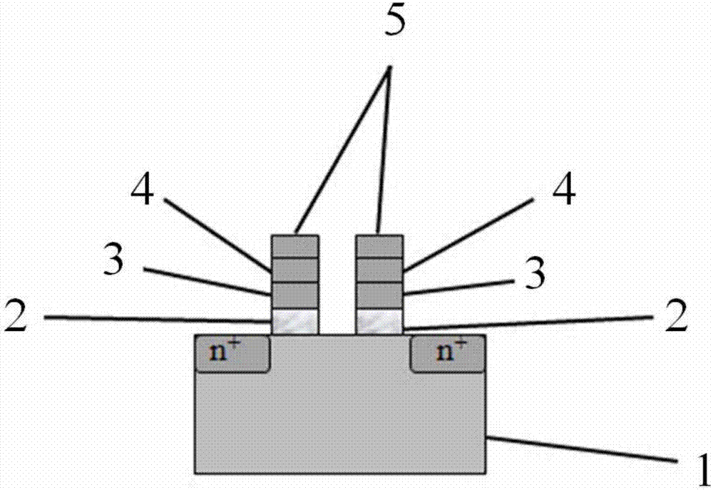
[0042]An embodiment of the hafnium oxide-based ferroelectric gate structure of the present invention includes a substrate, and a buffer layer, a bottom electrode layer, a ferroelectric storage layer and a top electrode layer are sequentially stacked on the surface of the substrate; wherein, The material of the substrate is P-type silicon; the material of the buffer layer is 3nm hafnium oxide; the material of the bottom electrode layer is 55nm TiN; the material of the ferroelectric storage layer is 15nm hafnium oxide doped with zirconium. The material ratio of the elements is: hafnium: zirconium = 1:1; the material of the top electrode is 20nm metal TiN.

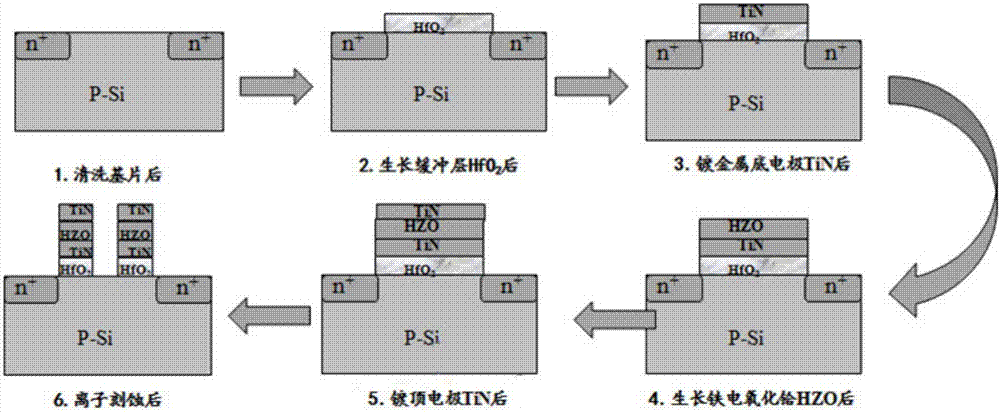
[0043] The preparation process of the ferroelectric gate structure based on hafnium oxide described in this embodiment, as shown in the attached figure 2 shown, including the following steps:

[0044] (1) Clean the P-type silicon with a standard cleaning process;

[0045] (2) A hafnium oxide buffer layer is formed on the P...

Embodiment 2

[0050] An embodiment of the ferroelectric grid structure based on hafnium oxide in the present invention includes a substrate, and a buffer layer, a bottom electrode layer, a ferroelectric layer and a top electrode layer are sequentially stacked on the surface of the substrate; wherein, the substrate The bottom material is N-type silicon; the buffer layer material is 5nm hafnium oxide; the bottom electrode layer material is 45nm metal TaN; the ferroelectric layer material is 18nm zirconium-doped hafnium oxide, in which hafnium and zirconium elements The ratio of the amount of substances is: hafnium: zirconium = 0.55:0.45; the material of the top electrode is 55nm metal TiN.

[0051] The preparation process of the hafnium oxide-based ferroelectric gate structure described in this embodiment includes the following steps:

[0052] (1) Clean the N-type silicon with a standard cleaning process;

[0053] (2) A hafnium oxide buffer layer is formed on the N-type silicon, and the hafn...

Embodiment 3

[0058] An embodiment of the ferroelectric grid structure based on hafnium oxide in the present invention includes a substrate, and a buffer layer, a bottom electrode layer, a ferroelectric layer and a top electrode layer are sequentially stacked on the surface of the substrate; wherein, the substrate The bottom material is P-type silicon; the buffer layer material is 7nm hafnium oxide; the bottom electrode layer material is 20nm metal TiN; the ferroelectric layer material is 16nm silicon-doped hafnium oxide, in which hafnium and silicon elements The ratio of the amount of substances is: hafnium:silicon=0.75:0.25; the material of the top electrode is 20nm TiN and 30nm Al.

[0059] The preparation process of the hafnium oxide-based ferroelectric gate structure described in this embodiment includes the following steps:

[0060] (1) Clean the P-type silicon with a standard cleaning process;

[0061] (2) A hafnium oxide buffer layer is formed on the P-type silicon, and the hafnium...


PUM

PropertyMeasurementUnit
thicknessaaaaaaaaaa
thicknessaaaaaaaaaa
thicknessaaaaaaaaaa

Abstract

The invention discloses a hafnium oxide based ferroelectric grid structure. The structure comprises a substrate, and a buffer layer, a bottom electrode layer, a ferroelectric layer and a top electrode layer are laminated on the surface of the substrate successively, and the material of the ferroelectric layer comprises hafnium oxide. The invention also discloses a preparation technology of the hafnium oxide based ferroelectric grid structure. The hafnium oxide based ferroelectric grid structure has high electrical performances, the vertical size of the whole storage medium of a ferroelectric memory is reduced by 10 to 20 times, and the structure and technology are compatible with the silicon technology.

Description

technical field [0001] The invention relates to a memory, in particular to a ferroelectric gate structure based on hafnium oxide and a preparation process thereof. Background technique [0002] Ferroelectric memory (FRAM) has been widely studied because of its high speed, non-volatility, low operating voltage, strong radiation resistance, and compatibility with standard silicon integrated circuit technology. Among them, the gate electrode / ferroelectric layer / buffer layer / substrate (MFIS) structure ferroelectric field effect transistor has become a research hotspot in the field of FRAM because of its non-destructive readout, simple structure and high storage density. However, in the MFIS structure, the dielectric constant and thickness of the I layer are required to be high, and when the dielectric constant of the buffer layer is small, the structure will cause most of the voltage to fall on the buffer layer, resulting in the failure of the ferroelectric layer to separate. L...

Claims


Application Information

Patent Timeline
Patent Type & Authority Applications(China)
IPC IPC(8): H01L29/51H01L21/28H01L29/78H01L21/336
CPCH01L29/40111H01L29/516H01L29/6684H01L29/78391
Inventor 彭强祥刘巧灵廖敏周益春
Owner XIANGTAN UNIV
Why Eureka
Try Eureka