
Ultra-Wideband Bandpass Filter Based on Parallel Coupled Lines

A technology of band-pass filter and parallel coupled lines, which is applied in the field of ultra-wideband band-pass filters, can solve the problems of complex design of coupled lines for terminal short circuit, small filter size, high insertion loss, etc., and achieve simple topology and space utilization The effect of high efficiency and improved selection performance

Inactive Publication Date: 2019-06-21
NANJING UNIV OF SCI & TECH
View PDF4 Cites 0 Cited by
  • Summary
  • Abstract
  • Description
  • Claims
  • Application Information

AI Technical Summary

Problems solved by technology

[0004] At present, the main methods of designing ultra-wideband filters at home and abroad are: (1) dual-mode and multi-mode resonator methods, this type of broadband / UWB bandpass filter design method is simple and compact; (2) cascaded low-pass-high-pass Or band-pass band-stop method, this type of ultra-wideband filter is large in size, does not meet the requirements of miniaturization, and has high insertion loss; (3) Hybrid microstrip / CPW method, although this method has a compact circuit size, However, because of the double-layer structure, special installation methods are required, which increases the complexity of its integration with the system;
[0005] In 2012, Wang Hui innovatively proposed a three-wire coupled resonator in the paper "UWB bandpass filter with novel structure and supercompact size", and used the three-wire coupled resonator to load stubs to realize an ultra-wideband filter. The filter has a very small size, but the passband selectivity still needs to be further improved
However, in this paper, the strong coupling of the coupling line is realized through the back gap and the defect ground (DGS) structure, and the design of the coupling line for terminal short circuit is relatively complicated.

Method used


Image

  • Ultra-Wideband Bandpass Filter Based on Parallel Coupled Lines
  • Ultra-Wideband Bandpass Filter Based on Parallel Coupled Lines
  • Ultra-Wideband Bandpass Filter Based on Parallel Coupled Lines

Examples


Embodiment

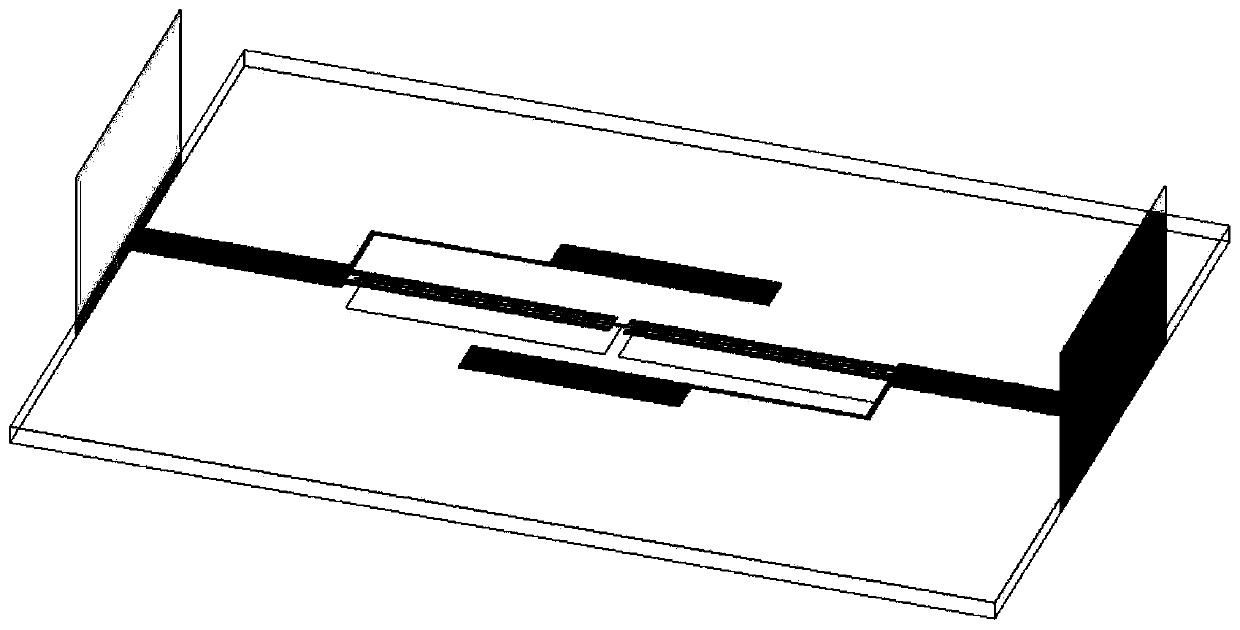
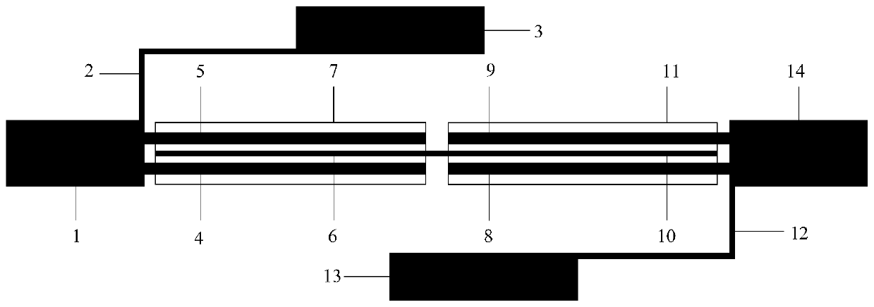
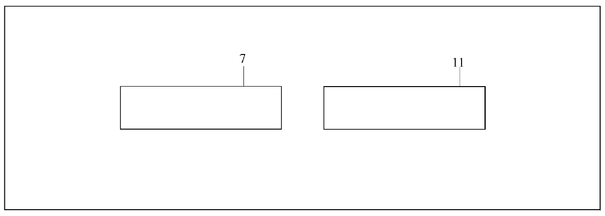
[0024] The structure of the UWB bandpass filter based on parallel coupled lines in this embodiment is as follows figure 1 As shown, the intermediate dielectric plate is Rogers 4003C, with a thickness of 0.508 mm, a relative dielectric constant of 3.55, and a loss tangent of 0.0027. Use the 3D electromagnetic simulation software HFSS based on the finite element method to optimize the structure of the high-selectivity ultra-wideband bandpass filter based on the stub-loaded ladder impedance resonator proposed by the present invention, and finally obtain the size of each microstrip line of the filter The parameters are as follows: the fourth microstrip line 4, the fifth microstrip line 5, the eighth microstrip line 8, and the ninth microstrip line 9 are all 7.55mm in length and 0.2mm in width; the sixth microstrip line 6, the The length of the tenth microstrip line 10 is 7.55mm, and the width is 0.1mm; the length of the second microstrip line 2 and the twelfth microstrip line 12 a...


PUM


Abstract

The invention discloses an ultra-wideband band-pass filter based on parallel coupling lines. The ultra-wideband band-pass filter comprises a dielectric substrate in the middle layer, a micro-strip structure positioned on the top layer of the dielectric substrate, a metal earth plate on the bottom layer and two input / output ports, wherein the micro-strip structure comprises a first parallel three-wire coupling line, a second parallel three-wire coupling line, a first branch knot loading step-impedance resonator and a second branch knot loading step-impedance resonator; the two input / output ports are connected with the two branch knot loading step-impedance resonators respectively; the metal earth plate comprises a first back gap unit and a second back gap unit, and the first gap unit and the second gap unit are arranged at the projection positions, on the metal earth plate, of the first parallel third-wire coupling line and the second parallel third-wire coupling line respectively. The ultra-wideband band-pass filter is simple in structure, compact in structure, convenient to process, stable in band-pass performance and relatively high in band-pass selectivity.

Description

technical field [0001] The invention relates to ultra-wideband filter technology, in particular to an ultra-wideband bandpass filter based on parallel coupled lines. Background technique [0002] In the "Tenth Five-Year Plan" 863 Plan communication technology theme research project released in early September 2001, the key technology of ultra-wideband wireless communication and its coexistence and compatibility technology were taken as the research content of wireless communication common technology and innovative technology, and domestic scholars were encouraged to strengthen this research and development work. In 2002, UWB wireless technology was approved by the Federal Communications Commission (FCC, Federal Communication Commission) for the first time, and can be used in short-distance wireless communication, which opened the door for the commercial application of UWB technology products and promoted the development of UWB systems. and the progress of its devices. As o...

Claims


Application Information

Patent Timeline
Patent Type & Authority Patents(China)
IPC IPC(8): H01P1/203H01P3/08
CPCH01P1/203H01P3/08
Inventor 杨国肖如奇王奕吴文
Owner NANJING UNIV OF SCI & TECH
Learn More