Stacked package structure and manufacturing method
A technology of packaging structure and manufacturing method, which is applied in semiconductor/solid-state device manufacturing, electrical components, electrical solid-state devices, etc., can solve the problems of thick stacking packaging structure, high manufacturing cost, complex process, etc., and achieves reduced thickness and reduced processing. Cost, effect of simplifying manufacturing process
- Summary
- Abstract
- Description
- Claims
- Application Information
AI Technical Summary
Problems solved by technology
Method used
Image

Examples
Embodiment 1
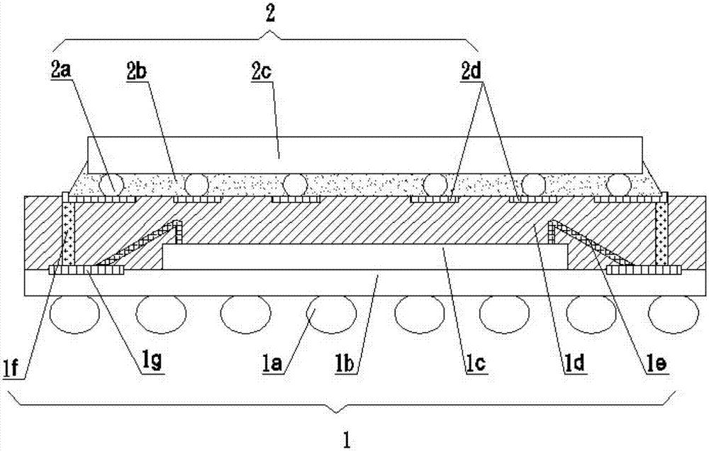
[0056] refer to figure 1 As shown, it is a structural schematic diagram of a preferred embodiment of the package-on-package structure of the present invention.
[0057] The package-on-package structure of this embodiment includes a first package 1 and a second package 2 stacked on the first package 1, wherein:
[0058] The first package body 1 includes a substrate 1b, and the substrate 1b has two opposite sides. A first component is mounted on one side of the substrate 1b and a first pad 1g is provided, and the first component is electrically connected to the first pad 1g through a first package circuit 1e. In a specific implementation, the first component may be a first chip 1c. The other surface of the substrate 1b is provided with first solder balls 1a for electrical connection with external components. The first package body 1 further includes a first glue injection body 1d covering the first component, the first solder pad 1g and the first package circuit 1e.
[0059]...
Embodiment 2
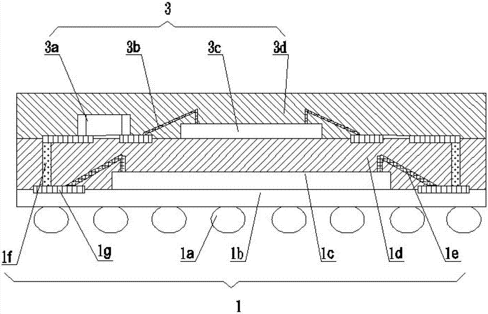
[0065] refer to figure 2 As shown, it is a structural schematic diagram of another preferred embodiment of the package-on-package structure of the present invention.
[0066] The package-on-package structure of this embodiment includes a first package body 1 and a third package body 3 stacked on the first package body 1, wherein
[0067] The structure of the first package body 1 is the same as that in the first embodiment, and will not be repeated here.
[0068] The third package body 3 includes a passive device, a third chip 3c, a second package circuit 3b electrically connecting the passive device and the third chip 3c, covering the passive device, the third chip 3c and the second package circuit 3b The third injection colloid 3d.
[0069] The third package 3 is attached to the first package 1 through the joint of the third glue 3d and the first glue 1d, and the first package circuit 1e and the second package circuit 3b are arranged on the first package 1d. The conductiv...
Embodiment 3
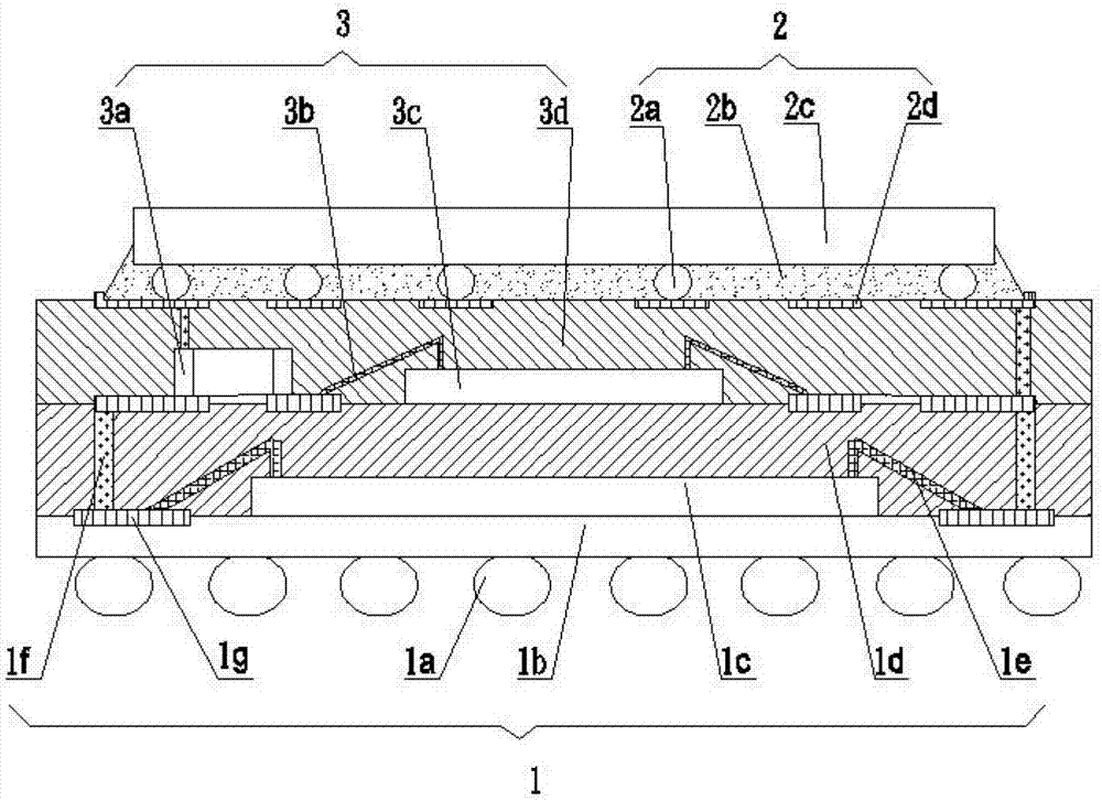
[0072] refer to image 3 As shown, it is a structural schematic diagram of another preferred embodiment of the package-on-package structure of the present invention.
[0073] The package-on-package structure of this embodiment includes a first package 1 , a third package 3 stacked on the first package 1 , and a second package 2 stacked on the third package 3 . The structures of the first package body 1 , the second package body 2 , and the third package body 3 are the same as those in the first and second embodiments. The third package body 3 is stacked on the first package body 1 in the same manner as in the second embodiment. The second package body 2 is stacked on the third package body 3 through the bonding of the second glue body 2b and the third glue body 3d.
[0074] It can be understood that, in specific implementation, more layers of stacking and packaging can be performed with reference to the stacking manner of Embodiment 3 according to actual needs.
[0075] Bas...
PUM
 Abstract
Description
Claims
Application Information
 - R&D
- Intellectual Property
- Life Sciences
- Materials
- Tech Scout
- Unparalleled Data Quality
- Higher Quality Content
- 60% Fewer Hallucinations
Browse by: Latest US Patents, China's latest patents, Technical Efficacy Thesaurus, Application Domain, Technology Topic, Popular Technical Reports.
© 2025 PatSnap. All rights reserved.Legal|Privacy policy|Modern Slavery Act Transparency Statement|Sitemap|About US| Contact US: help@patsnap.com