Ultra-fast biasing temperature instability test system and method applied to semiconductor device

A technology of bias temperature and instability, which is applied in the direction of single semiconductor device testing, instrumentation, and electrical measurement. It can solve the problems of slow recovery effect and inability to accurately characterize the BTI characteristics of devices, so as to achieve accurate measurement and high test sensitivity. Effect

Active Publication Date: 2017-09-15
ZHEJIANG UNIV
View PDF7 Cites 13 Cited by
  • Summary
  • Abstract
  • Description
  • Claims
  • Application Information

AI Technical Summary

Problems solved by technology

In the existing test method of BTI characteristic, adopt traditional direct current voltage test method to obtain MOSFET transistor drain current I d vs. gate voltage V g The output transfer characteristic curve to find the threshold voltage, usually takes about a few seconds
However, using on-the-fly or other

Method used


Image

  • Ultra-fast biasing temperature instability test system and method applied to semiconductor device
  • Ultra-fast biasing temperature instability test system and method applied to semiconductor device
  • Ultra-fast biasing temperature instability test system and method applied to semiconductor device

Examples


Embodiment Construction

[0024] The following introductions are some of the possible embodiments of the present invention, which are intended to provide a basic understanding of the present invention, and are not intended to identify key or decisive elements of the present invention or limit the scope of protection. It is easy to understand that, according to the technical solution of the present invention, those skilled in the art may propose other alternative implementation manners without changing the essence and spirit of the present invention. Therefore, the following specific embodiments and drawings are only exemplary descriptions of the technical solution of the present invention, and should not be regarded as the entirety of the present invention or as a limitation or limitation on the technical solution of the present invention.

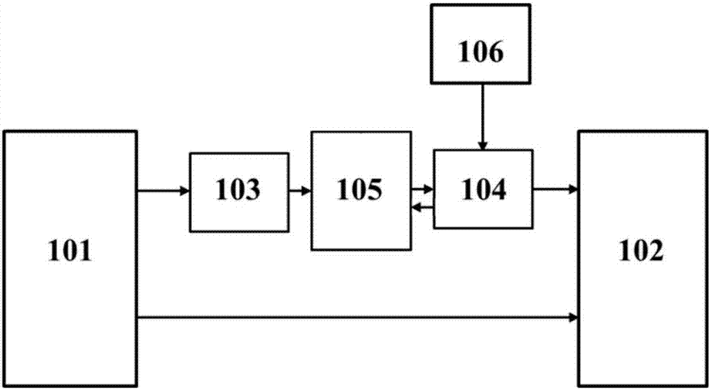
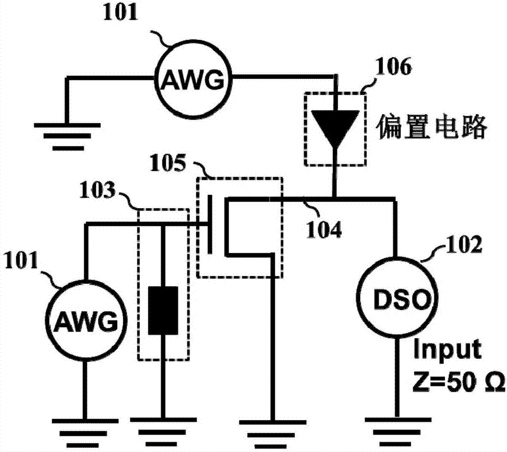
[0025] Such as figure 1 As shown, an ultra-fast bias temperature instability test system applied to semiconductor devices includes an arbitrary waveform generator ...


PUM


Abstract

The invention discloses an ultra-fast biasing temperature instability test system and method applied to a semiconductor device. The system comprises an arbitrary waveform generator, a waveform processor, an input probe, an output probe and a drain bias module. The arbitrary waveform generator generates a stress voltage signal, a restore voltage signal and a measuring voltage signal that have precisely controllable levels and time; and a gate voltage signal is loaded at a gate of a measured device by the input probe. According to the invention, the voltage amplitude and time that can generate a BTI effect can be controlled precisely; the BTI effect in extremely short time can be represented; and the test sensitivity is high. The representation of a threshold voltage drift can be realized in very short time; the test result is little affected by a restoring effect of a BTI effect; and thus accurate measurement is realized. The system and method can be applied to electrical characteristic studies of high-performance planar transistors using silicon, germanium, III-V class compounds as carrier channels, a fin-type three-dimensional gate, a field-effect transistor having a ring-gate (GAA) structure.

Description

technical field [0001] The invention belongs to the technical field of characterization and testing of the reliability of semiconductor devices, in particular to a method for controlling the bias temperature of high-performance electronic devices, especially Metal Oxide Semiconductor Field Effect Transistors (MOSFETs) within a very short time (<10ns). Stability Characterization Techniques. Background technique [0002] In the past few decades, with the development of CMOS integrated circuit technology, the size of the core unit in the circuit - metal oxide semiconductor field effect transistors (MOSFETs) has gradually decreased in accordance with Moore's law, from a few microns (μm) to 14nm , The density and performance of transistor devices continue to increase. One of the important indicators to measure the reliability of transistor devices is the bias temperature instability (BTI) of semiconductor devices. Bias temperature instability includes negative bias temperatu...

Claims


Application Information

Patent Timeline
IPC IPC(8): G01R31/26
CPCG01R31/2628
Inventor 赵毅玉虓陈冰曲益明
Owner ZHEJIANG UNIV
Why Eureka
Try Eureka