
Flexible conducting film and preparing method thereof

A technology of flexible conductive and conductive layers, which is applied to equipment for manufacturing conductive/semiconductive layers, chemical instruments and methods, cable/conductor manufacturing, etc. It can solve the problems of poor shadow elimination effect and achieve good shadow elimination effect , wide applicability

Pending Publication Date: 2017-09-15
CSG HOLDING +1
View PDF11 Cites 0 Cited by
  • Summary
  • Abstract
  • Description
  • Claims
  • Application Information

AI Technical Summary

Problems solved by technology

[0003] Based on this, it is necessary to provide a flexible conductive film and a preparation method thereof for the problem that the shadow elimination effect is not good when the square resistance of the ITO conductive film in the flexible conductive film is low.

Method used

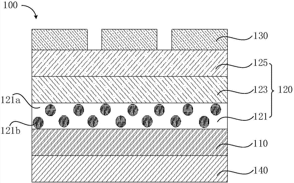
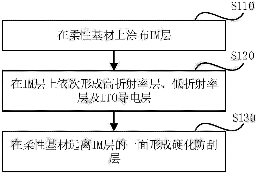

Image

  • Flexible conducting film and preparing method thereof
  • Flexible conducting film and preparing method thereof
  • Flexible conducting film and preparing method thereof

Examples


preparation example Construction

[0054] see figure 2 , the preparation method of the flexible conductive film of an embodiment comprises the following steps:

[0055] S110, coating the IM layer on the flexible substrate.

[0056] In one embodiment, the IM layer is coated on the flexible substrate by wet coating.

[0057] In one embodiment, the flexible substrate is sheet-shaped; the thickness of the flexible substrate is 50 μm˜125 μm. Preferably, the thickness of the flexible substrate 110 is 50 μm, 100 μm or 125 μm.

[0058] In one of the embodiments, the material of the flexible substrate is selected from polyethylene terephthalate (PET), cycloolefin polymer (COP), cycloolefin copolymer (COC), polycarbonate (PC) and At least one of cellulose triacetate (TAC).

[0059] In one embodiment, the thickness of the IM layer is 0.8 μm˜3 μm or 35 nm˜42 nm. In one of the embodiments, when the thickness of the IM layer is 0.8 μm to 3 μm, the IM layer also has the function of a hardening layer, which can improve t...

Embodiment 1

[0079] An optical-grade PET film with a thickness of 125 μm is selected as the flexible substrate; the IM layer is coated on the flexible substrate by wet coating, and the IM layer contains ZrO 2 Epoxy acrylate coating of high refractive index particles, the thickness of the IM layer is 1.0 μm, and the refractive index of the IM layer is 1.62; then a high refractive index layer is formed on the IM layer by magnetron sputtering, and the high refractive index layer TiO 2 layer, the thickness of the high refractive index layer is 6.5nm, and the refractive index of the high refractive index layer is 2.6; then a low refractive index layer is formed on the high refractive index layer by magnetron sputtering, and the low refractive index layer is SiO 2 layer, the thickness of the low refractive index layer is 30nm, and the refractive index of the low refractive index layer is 1.46; then on the low refractive index layer, an ITO conductive layer is formed by magnetron sputtering, the ...

Embodiment 2

[0081] An optical-grade TAC film with a thickness of 125 μm is selected as the flexible substrate; the IM layer is coated on the flexible substrate by wet coating, and the IM layer contains ZrO 2 Polyurethane acrylate coating of high refractive index particles, the thickness of the IM layer is 1.0 μm, and the refractive index of the IM layer is 1.67; then a high refractive index layer is formed on the IM layer by magnetron sputtering, and the high refractive index layer is Si 3 N 4 layer, the thickness of the high refractive index layer is 23nm, and the refractive index of the high refractive index layer is 1.9; then a low refractive index layer is formed on the high refractive index layer by magnetron sputtering, and the low refractive index layer is SiO 2 layer, the thickness of the low refractive index layer is 18nm, and the refractive index of the low refractive index layer is 1.46; then on the low refractive index layer, an ITO conductive layer is formed by magnetron spu...


PUM

PropertyMeasurementUnit
thicknessaaaaaaaaaa
thicknessaaaaaaaaaa
thicknessaaaaaaaaaa

Abstract

The invention relates to a flexible conducting film and a preparation method thereof. The flexible conducting film includes a flexible base material, a refraction composite layer and an ITO conducting layer which are successively laminated. The refraction composite layer is composed of an IM layer, a high refraction rate layer and a lower refraction rate layer which are successively laminated. The flexible base material is selected from at least one of the PET, COP, COC, PC and TAC. The IM layer includes an organic resin coating and high refraction rate particles, has a thickness of 0.8[mu]m-3[mu]m or 35nm-42nm. The high refraction rate layer material is selected from at least one of Nb205, Ti02 and Si3N4, and has a thickness of 3.5nm-24nm. The low refraction rate layer material is selected from at least one of the SiO2 and SiOxNy, and has a thickness of 7nm-38nm. The ITO conducting layer is subject to aging processing and obtains a square resistance of 45[omega]-50[omega]. The flexible conducting film defines the material and the thickness of the IM layer, the high refraction rate layer and the lower refraction rate layer, such that the ITO conducting layer obtains a square resistance of 45[omega]-50[omega] after being subject to aging processing. The flexible conducting film has better disapparate effects.

Description

technical field [0001] The invention relates to the technical field of preparation of flexible conductive materials, in particular to a flexible conductive film and a preparation method thereof. Background technique [0002] Indium tin oxide (ITO) film, as the most commonly used transparent conductive film, is widely used in the field of transparent display. The square resistance of the ITO conductive layer in the conventional flexible conductive film on the market is 150±20 ohms. In order to eliminate the shadow of the ITO electrode after etching, an organic IM layer with a high refractive index is often coated on the flexible substrate first, and then deposited by SiO 2 and other low refractive index optical matching layers, and finally deposit the ITO conductive layer, so as to reduce the color difference between the ITO area and the ITO etching area, and finally realize the disappearance. However, with the development of the touch screen industry, the size of the produc...

Claims


Application Information

Patent Timeline
Patent Type & Authority Applications(China)
IPC IPC(8): H01B5/14H01B13/00B32B27/06B32B3/14B32B33/00
CPCH01B5/14H01B13/0026B32B3/14B32B27/06B32B33/00
Inventor 马志锋杜晓峰孙官恩张莉
Owner CSG HOLDING
Learn More