Method for taking out chip from package

A package and chip technology, applied in the direction of single semiconductor device testing, semiconductor/solid-state device manufacturing, electrical components, etc., can solve problems such as long time, inability to perform secondary bonding, aluminum PAD corrosion, etc., to reduce thermal damage, Avoid strong acid to corrode the chip, and the treatment effect is consistent

Inactive Publication Date: 2017-09-15
BEIJING SMARTCHIP MICROELECTRONICS TECH COMPANY +3
View PDF3 Cites 3 Cited by
  • Summary
  • Abstract
  • Description
  • Claims
  • Application Information

AI Technical Summary

Problems solved by technology

In the implementation of this method, concentrated sulfuric acid needs to gradually and slowly infiltrate through the gap between the chip and the ceramic substrate to achieve the purpose of corrosion. It takes a long time, and too long time will cause corrosion of the aluminum PAD, making it impossible to perform secondary bonding.

Method used


Image

  • Method for taking out chip from package
  • Method for taking out chip from package
  • Method for taking out chip from package

Examples


Embodiment Construction

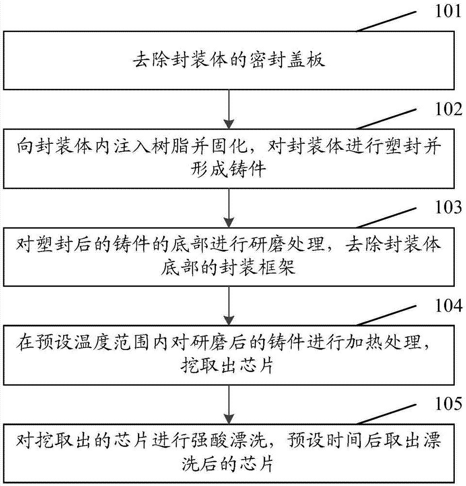
[0042] The specific embodiments of the present invention will be described in detail below in conjunction with the accompanying drawings, but it should be understood that the protection scope of the present invention is not limited by the specific embodiments.

[0043] According to an embodiment of the present invention, a method for taking out a chip from a package is provided, figure 1 It is a flowchart of the method, specifically including steps 101-105:

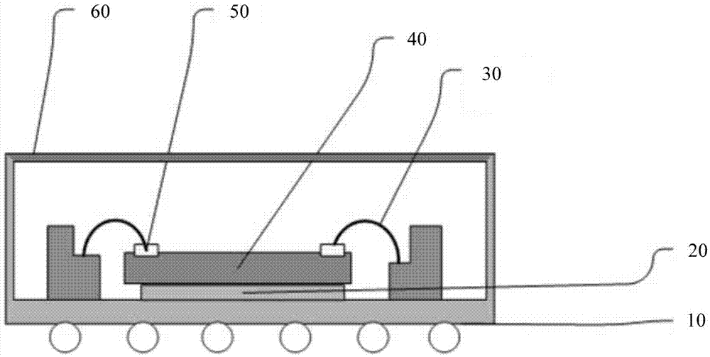
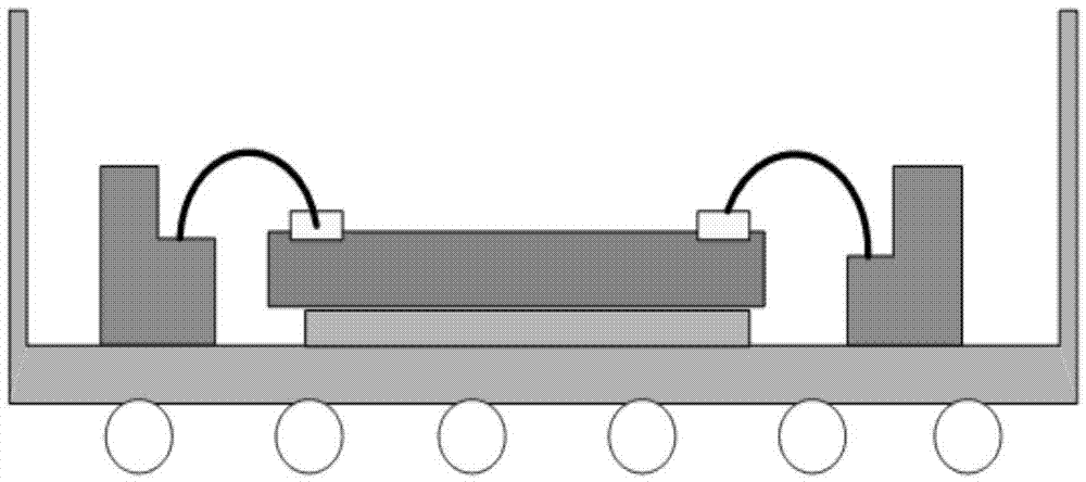
[0044] Step 101 : remove the sealing cover of the package, the package frame is provided at the bottom of the package, and the chip is arranged on the package frame through the adhesive, and the sealing cover is provided on the upper part of the package.

[0045] In the embodiment of the present invention, the package body adopts a metal or ceramic package frame 10 , and the die-bonding adhesive 20 can specifically adopt silver paste, eutectic solder, or conductive adhesive. For details, see figure 2 As shown, the pack...


PUM


Abstract

The invention discloses a method for taking out a chip from a package. The method comprises the following steps: removing a sealing cover plate of the package, wherein a packaging frame is arranged at the bottom of the package, a chip is arranged on the packaging frame through an adhesive tape glue, and the sealing cover plate is arranged at the upper part of the package; injecting resin into the package and curing, carrying out plastic packaging on the package and forming a casting; carrying out grinding treatment at the bottom of the casting after plastic packaging, and removing the packaging frame at the bottom of the package; carrying out heating treatment on the casting after grinding in a preset temperature range, and taking out the chip; and carrying out strong acid rinsing on the chip taken out, and taking out the chip after rinsing after reset time. According to the method, the chip can be taken out from the package without heating at too high temperature; and moreover, the acid treatment time is relatively short, a bonding pad cannot be corroded, the chip can be taken out completely, and the chip can also be packaged at second time.

Description

technical field [0001] The invention relates to the technical field of integrated circuit manufacturing, in particular to a method for taking out a chip from a package. Background technique [0002] As the core component of the product, the chip's performance and quality have a crucial impact on the final quality of the product. In the chip design stage or in the process of use, failure analysis is required after the chip fails. Usually, the process is to conduct electrical failure analysis first, and then perform physical failure analysis according to the preliminary analysis conclusion. During physical failure analysis, the package or chip needs to be destroyed. To observe the location and phenomenon of failure. In the research and development stage, in order to save costs, the form of MPW (Multi Project Wafer) is often used for tape-out. Chips are especially precious due to the small number, or for some specific failure situations, it is necessary to repair the circuit a...

Claims


Application Information

Patent Timeline
IPC IPC(8): H01L21/00G01R31/26
CPCG01R31/26H01L21/00
Inventor 李建强单书珊陈燕宁张海峰唐晓柯赵东艳章姝俊
Owner BEIJING SMARTCHIP MICROELECTRONICS TECH COMPANY
Why Eureka
Try Eureka