A crystallization method and device based on solution flow
A solution and crystallization technology, applied in chemical instruments and methods, solutions from liquid solvents at room temperature, single crystal growth, etc., can solve the problems of troublesome solution flow, complex devices, high energy consumption, etc., and achieve good universality and simple process , the effect of good application prospects
- Summary
- Abstract
- Description
- Claims
- Application Information
AI Technical Summary
Problems solved by technology
Method used
Image
Examples
Embodiment approach
[0034] According to a preferred embodiment of the present invention, the substrate (or substrate) sample is also treated, which mainly refers to hydrophilic treatment or wettability treatment, to obtain a substrate with suitable wettability, for example, the substrate (or substrate) can be Bottom) The sample is placed under surface plasma (plasma) for a certain period of time, for example, for 1 minute to 5 hours, preferably for 2 minutes to 1 hour, more preferably for 5 minutes to 30 minutes. The substrate (or substrate) sample surface is made solvent-affinic. Taking another way as an example, sulfuric acid and hydrogen peroxide solution can be mixed in a certain ratio, the preferred ratio is 7:3 or 6:4, at a certain temperature, preferably 20-120°C, and the sample is treated for a certain period of time. This treatment time is preferably 20-120 minutes.
[0035] Step 2, selecting a solvent and a solute, and optionally adding the solute to the solvent to form a solution.
...
Embodiment 1
[0067] use as Figure 5 The crystallization setup shown,
[0068] Select a silicon wafer with a silicon oxide layer with a thickness of 300nm-320nm on the surface as the substrate 1, and perform hydrophilic treatment on it, that is, place the sample under surface plasma treatment for 10 minutes;
[0069] Choose N,N-dimethylformamide as solvent, CH 3 NH 3 PB 3 Perovskite material precursors (CH 3 NH 3 I and PbI 2 Molar ratio 1:1)) is a solute, after forming a solution, the solution is added dropwise to the surface of the substrate, and under the action of affinity, the solution spreads on the surface of the substrate;
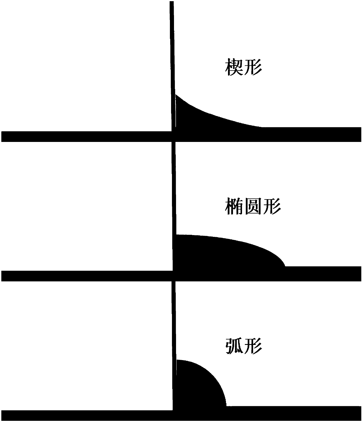
[0070] Select a glass sheet without affinity treatment as the vertical sheet 2, place it vertically on the surface of the substrate spread with the solution 3, and form a wedge-shaped solution area at the junction of the vertical sheet and the substrate;
[0071] Then apply a heat source above the above system, and refrigerate below, and obtain an ultra-l...
Embodiment 2
[0073] Carry out crystallization as in Example 1, the difference is that Si / SiO is selected respectively 2 , glass, mica, PET (polyethylene terephthalate), FTO, ITO as the substrate, N,N-dimethylformamide as the solvent, and the perovskite material (CH 3 NH 3 PB 3 ) solute, select Si / SiO without affinity treatment 2 , glass, mica, PET, FTO, and ITO as vertical sheets, after applying a temperature field, a millimeter-scale perovskite crystal array structure is obtained, such as Figure 6 , where (a) corresponds to Si / SiO 2 , (b) corresponds to glass, (c) corresponds to mica, (d) corresponds to PET, (e) corresponds to FTO, (f) corresponds to ITO.
PUM
| Property | Measurement | Unit |
|---|---|---|
| thickness | aaaaa | aaaaa |
Abstract
Description
Claims
Application Information


