Light-emitting device, pixel defining layer and manufacturing method thereof

A technology of pixel definition layer and definition layer, which is applied in the manufacture of semiconductor/solid-state devices, electric solid-state devices, semiconductor devices, etc., can solve the problems of inability to meet, affect the display effect, and the transparent pixel definition layer cannot block lateral outgoing, so as to achieve blocking side effect

Active Publication Date: 2017-09-26
TCL CHINA STAR OPTOELECTRONICS TECH CO LTD
View PDF7 Cites 19 Cited by
  • Summary
  • Abstract
  • Description
  • Claims
  • Application Information

AI Technical Summary

Problems solved by technology

This means that not only in the vertical direction, but also in the horizontal direction, it is possible for QD to emit light. On the one hand, this characteristic is beneficial to the improvement of the viewing angle of LCD by QDCF materials, but on the other hand, it will lead to differences in the CF photoresist layer. Lateral excitation between, such as figure 2 , when the green QD color-resistor 101 emits light, the transparent pixel def

Method used


Image

  • Light-emitting device, pixel defining layer and manufacturing method thereof
  • Light-emitting device, pixel defining layer and manufacturing method thereof
  • Light-emitting device, pixel defining layer and manufacturing method thereof

Examples


Embodiment Construction

[0042] In order to enable those skilled in the art to better understand the technical solutions of the present invention, the present invention will be further described in detail below in conjunction with the accompanying drawings and specific embodiments.

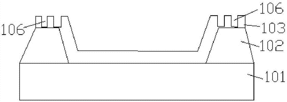
[0043] Please refer to figure 1 , the pixel defining layer in Embodiment 1 of the present invention includes a dam body 102 disposed on a substrate 101 as the first defining layer, and the dam body 102 in this embodiment adopts a common defining layer material, which does not require lyophilicity characteristics; then the metal layer 103 is set above the base 101 and the dam body 102, as the second delimiting layer, specifically a layer of metal film that is coherently arranged on the base 101 and the dam body 102 side walls and the top, and is positioned at the top of the dam body 102 The surface of the metal layer 103 has a nano-microstructure 106, which meets the hydrophobicity requirements of the upper part of the pi...


PUM

PropertyMeasurementUnit
Sizeaaaaaaaaaa

Abstract

The invention discloses a pixel defining layer which comprises a first defining layer and a second defining layer, wherein the first defining layer comprises dam bodies; the second defining layer comprises metal layers arranged on the side walls/part of the side walls of the tops of the dam bodies; the surfaces of the metal layers located at the tops of the dam bodies are of nano microstructures. The invention further provides a light-emitting device. A manufacturing method I comprises the following steps: preparing the second defining layer on the dam bodies, preparing a photoresist layer with the nano microstructure on the surface on the second defining layer through a nano imprinting procedure, and enabling the surface of the second defining layer on the tops of the dam bodies to be of the nano microstructure through an etching procedure. A manufacturing method II comprises the following steps: preparing the second defining layer with the nano microstructure on the surface on a substrate and the first defining layer in a grazing incidence depositing mode, and removing the second defining layer, which is located between the dam bodies, above the substrate through the etching procedure. The pixel defining layer disclosed by the invention can resist lateral light leakage to enable emergent light energy to be increased; the nano microstructures of the metal layers have dewatering characteristics, thus guaranteeing the reliability of ink dripping.

Description

technical field [0001] The invention relates to the field of display technology, in particular to a light emitting device, a pixel defining layer therein and a manufacturing method thereof. Background technique [0002] Due to the advantages of self-illumination, no need for backlight, high contrast, thin thickness, wide viewing angle, fast response speed, and flexible panels, OLED displays are considered to be the next-generation flat-panel display emerging application technology. [0003] In the OLED technology, it is necessary to use organic or inorganic materials to make the pixel defining layer, so as to limit the organic material used for light emission in the sub-pixel area defined by the pixel defining layer, so as to realize high resolution and full-color display. OLED is a self-luminous device, and its light-emitting layer is very thin. In the overlapping region of cathode and anode, carriers pass through the recombination transition of electron-hole pairs to gener...

Claims


Application Information

Patent Timeline
IPC IPC(8): H01L27/32H01L51/52H01L51/56
CPCH10K59/122H10K50/856H10K71/00
Inventor 陈黎暄
Owner TCL CHINA STAR OPTOELECTRONICS TECH CO LTD
Why Eureka
Try Eureka