

Light emitting element and electron beam deposition apparatus for manufacturing same
An electron beam deposition and light-emitting element technology, which is applied in the manufacture of semiconductor/solid-state devices, electrical components, circuits, etc., can solve the problems of thick substrates or metal supports, inability to form ultra-thin pixels, and performance degradation of small light-emitting elements, etc. To achieve the effect of improved ladder coverage
- Summary
- Abstract
- Description
- Claims
- Application Information
AI Technical Summary
Problems solved by technology
Method used
Image

Examples
Embodiment Construction
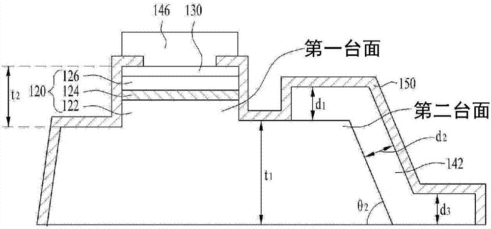
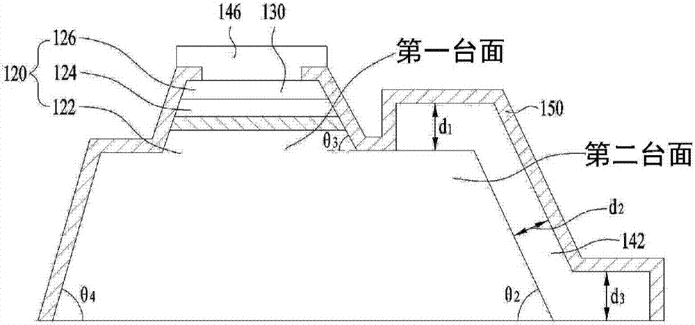
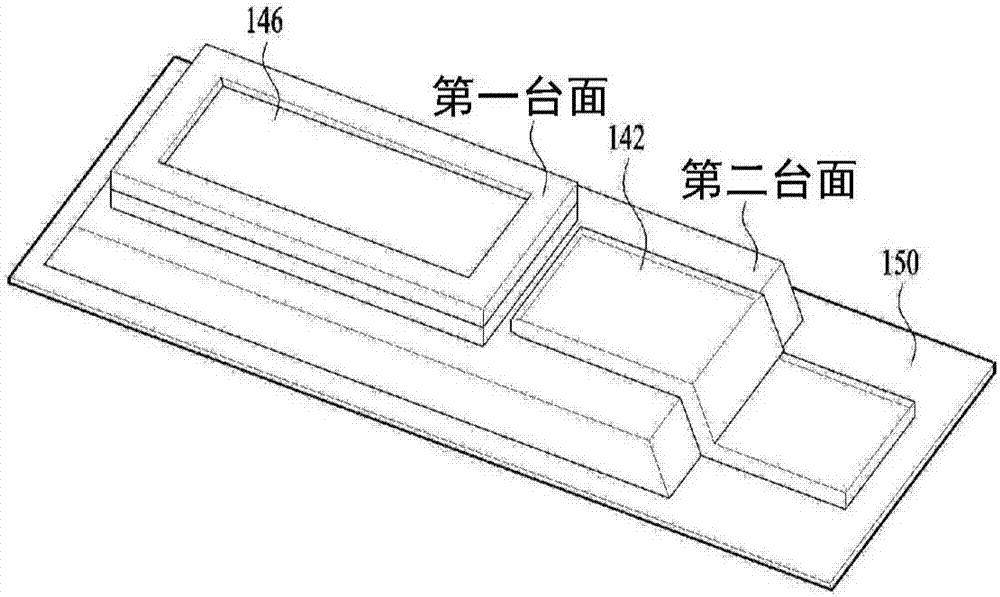
[0031] Hereinafter, the embodiments will be described in detail with reference to the accompanying drawings, so as to specifically achieve the above-mentioned objects.
[0032] In the description of the embodiments disclosed herein, it should be understood that when an element is referred to as being formed "on" or "under" another element, it can mean directly being "on" or "under" the other element. Or it is indirectly formed "above" or "below" other elements, with one or more elements interposed therebetween. It should also be understood that “on” or “under” an element may be described with respect to the drawings.
[0033] In addition, for example, related terms such as "first", "second", "above / upper / above" and "below / lower / below" used in the following description can be used to distinguish any substance or element from Another substance or element without requiring or containing any physical or logical relationship or sequence between these substances or elements.
[0034] In ...
PUM
 Abstract
Description
Claims
Application Information