Method and device for laser processing wafer

A laser processing and wafer technology, which is applied in metal processing, laser welding equipment, metal processing equipment, etc., can solve the problems of inability to use processing at the same time, and cannot form circular through holes, etc., so as to improve the effect and uniformity of laser processing High, uniform groove effect

Active Publication Date: 2018-11-09
北京中科镭特电子有限公司
View PDF5 Cites 0 Cited by
  • Summary
  • Abstract
  • Description
  • Claims
  • Application Information

AI Technical Summary

Problems solved by technology

Therefore, for example, in the case of penetrating a through hole in a semiconductor device etc., it is impossible to form a circular through hole.
Therefore, the processing of elliptical spot and circular spot cannot be used at the same time.

Method used


Image

  • Method and device for laser processing wafer
  • Method and device for laser processing wafer
  • Method and device for laser processing wafer

Examples


Embodiment Construction

[0059] In order to make the purpose, technical solutions and advantages of the embodiments of the present invention clearer, the technical solutions in the embodiments of the present invention will be clearly and completely described below in conjunction with the drawings in the embodiments of the present invention. Obviously, the described embodiments It is only some embodiments of the present invention, but not all embodiments. Based on the embodiments of the present invention, all other embodiments obtained by persons of ordinary skill in the art without making creative efforts belong to the protection scope of the present invention.

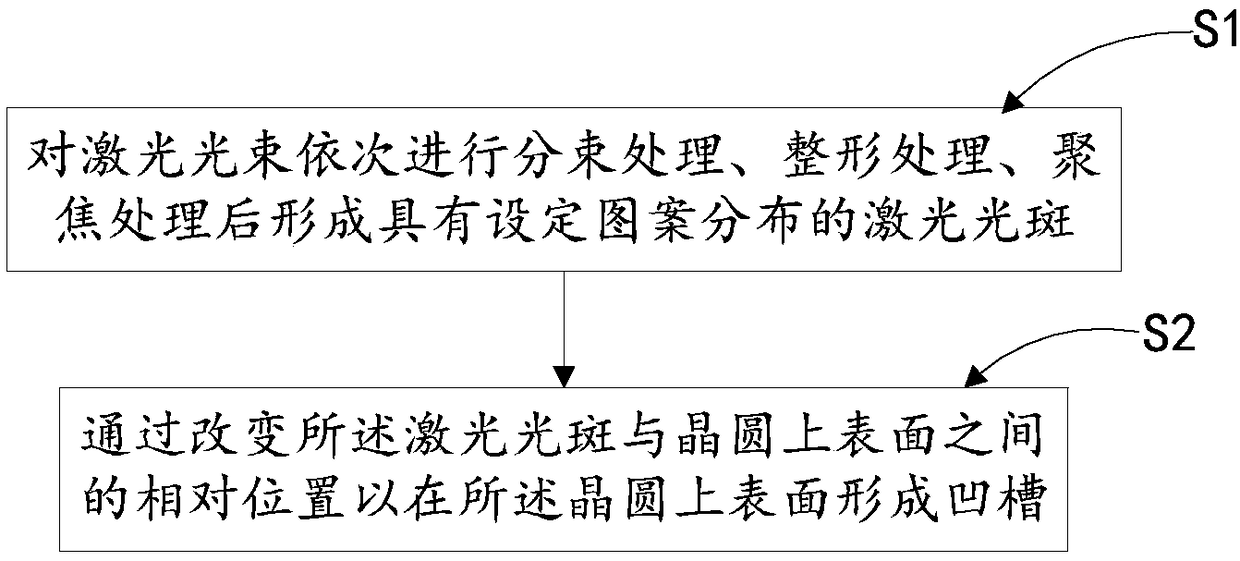
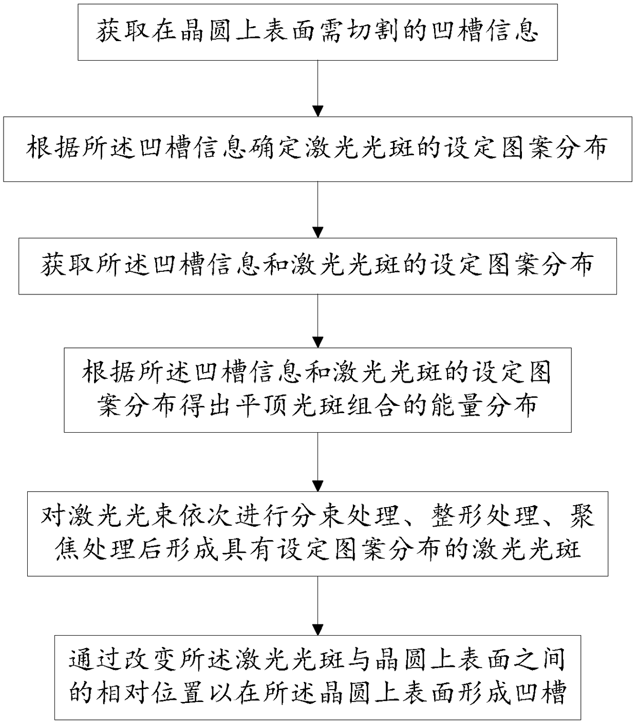
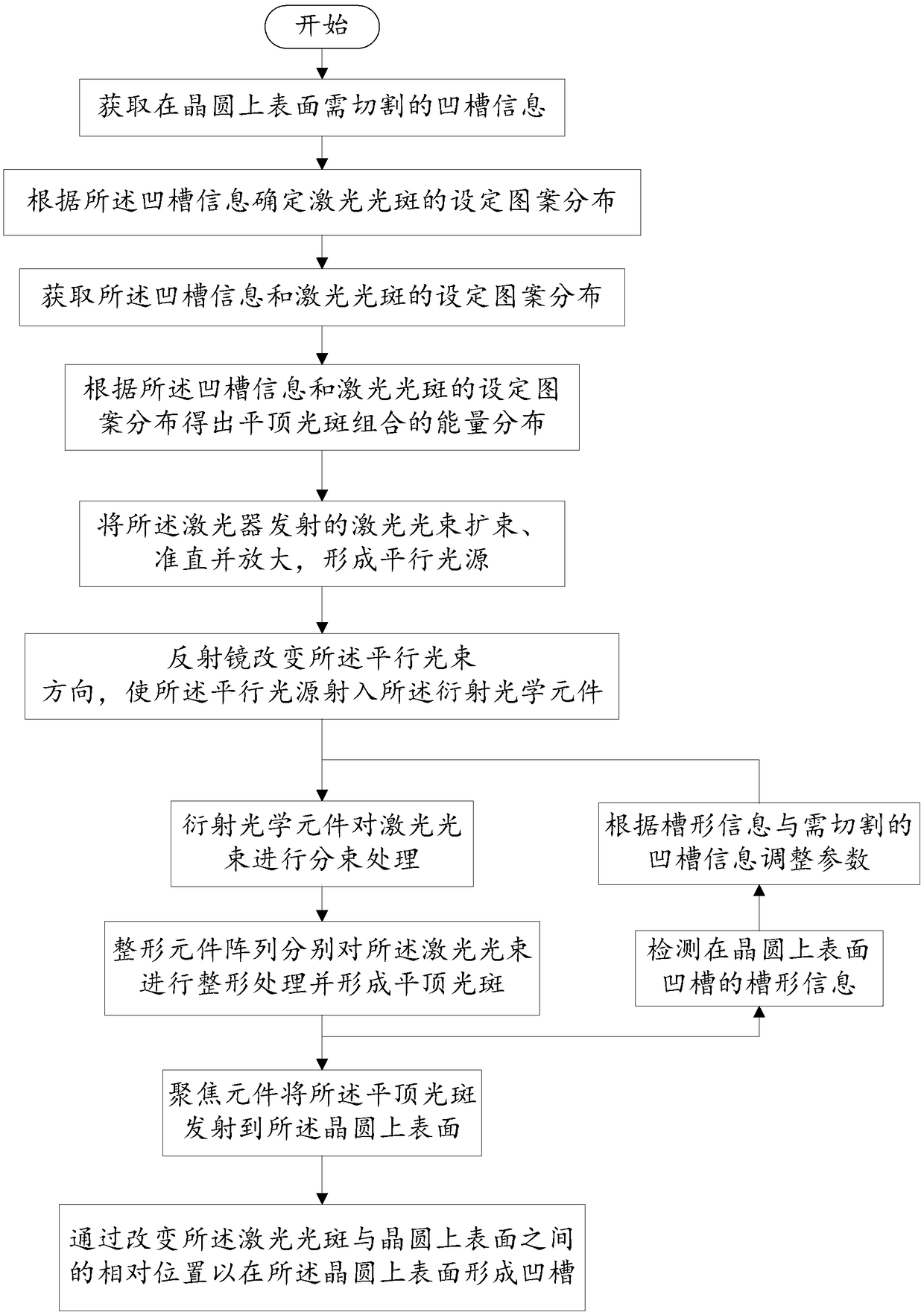
[0060] Embodiments of the present invention provide a method for laser processing wafers, such as figure 1 As shown, the method includes:

[0061] S1. The laser beam is sequentially subjected to beam splitting processing, shaping processing, and focusing processing to form a laser spot with a set pattern distribution;

[0062] S2. Forming g...


PUM


Abstract

The invention provides a method and device for machining wafers through laser. The method comprises the steps that after beam splitting treatment, shaping treatment and focusing treatment are sequentially carried out on laser beams, laser spots with set pattern distribution are formed; and space positions of the laser spots are adjusted so that grooves can be formed in the upper surfaces of the wafers. According to the method and the device, in the wafer laser machining process, according to the characteristic of the grooves, the laser beams are matched to the optimal set pattern distribution, energy of the scribed laser beams can be distributed more uniformly, the grooves formed in the upper surfaces of the wafers are more uniform, the heat influence area is smaller, uniformity is higher, and then the laser machining effect on the upper surfaces of the wafers is improved.

Description

technical field [0001] The invention relates to the fields of chip manufacturing and packaging and testing, in particular to a method and device for laser processing wafers. Background technique [0002] In recent years, with the continuous reduction of the feature size of semiconductor devices and the continuous improvement of chip integration, the parasitic capacitance between metal interconnections and multilayer wiring and the resistance of metal wires have increased sharply, resulting in RC delays, A series of problems such as increased power consumption limit the development of high-speed electronic components. When the feature size of the device is less than 90nm, the wafer must use a low dielectric constant material (hereinafter referred to as "Low-K") material instead of the traditional SiO 2 Layer (K ​​= 3.9 ~ 4.2), commonly used Low-K materials include Dow Corning's FOx and porous SiLK materials, Applied Materials' black diamond series low-K thin film materials, ...

Claims


Application Information

Patent Timeline
Patent Type & Authority Patents(China)
IPC IPC(8): B23K26/364B23K26/38B23K26/06B23K26/064B23K26/073
CPCB23K26/06B23K26/064B23K26/0643B23K26/073B23K26/364B23K26/38B23K2101/40
Inventor 刘嵩侯煜张紫辰
Owner 北京中科镭特电子有限公司
Why Eureka
Try Eureka