Packaging structure of UVLED lamp and UVLED lamp
A packaging structure and lamp holder technology, applied in electrical components, electrical solid devices, circuits, etc., can solve the problems of complex process and poor anti-aging performance, improve mechanical strength, avoid glue layer aging, and increase optional range. Effect
- Summary
- Abstract
- Description
- Claims
- Application Information
AI Technical Summary
Problems solved by technology
Method used
Image
Examples
Embodiment 1
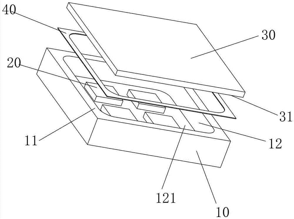
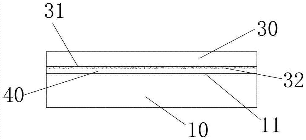
[0018] see figure 1 and figure 2 , the present invention relates to a packaging structure for UV LED lamps, including a lamp holder 10, four UV chips 20 and a glass cover 30 for covering the lamp holder 10, the top surface 11 of the lamp holder 10 is concave downward There is a groove 12, and four UV chips 20 are arranged in a rectangular array on the bottom surface 121 of the groove 12, and then each UV chip 20 is encapsulated by UV LED chip fusion glass, and the UV LED chip and the lamp holder 10 are electrically connected. connect.
[0019] The glass cover plate 30 is bonded and covered on the top surface 11 of the lamp holder 10 through an adhesive layer 40, and a metal film layer 32 is plated on the lower surface 31 of the glass cover plate 30 corresponding to the adhesive layer 40. In this embodiment, Metal film layer 32 adopts aluminum film layer, and the thickness of aluminum film layer is controlled at 3-5 microinch; In order to meet the requirement that the alumi...
Embodiment 2
[0021] The structure of this embodiment is substantially the same as that of Embodiment 1, the same structure will not be described in detail, and only the differences will be described. In this embodiment, the metal film layer 32 is a gold film layer, and the thickness of the gold film layer is controlled at 1-3 microinches. The shape and size of the gold film layer meet the requirement of covering the adhesive layer 40 to block the irradiation of ultraviolet light on the adhesive layer 40 .
[0022] It should be noted that the adhesive layer 40 of the present invention can also be an inorganic material adhesive layer, and the metal film layer 32 is plated on the lower surface 31 of the glass cover 30 to increase the optional range of adhesive layer materials.
PUM
 Abstract
Description
Claims
Application Information

