Die taking and die bonding device and die bonding machine employing same

A technology of die bonding and driving device, which is applied in semiconductor/solid-state device manufacturing, electrical components, circuits, etc., and can solve the problems of chip voiding, uneven temperature control, and high energy consumption

Active Publication Date: 2017-10-13
SUZHOU ACCURACY ASSEMBLY AUTOMATION CO LTD
View PDF4 Cites 11 Cited by
  • Summary
  • Abstract
  • Description
  • Claims
  • Application Information

AI Technical Summary

Problems solved by technology

[0003] For chips with a DAF film on the back, the package size is the same as the chip size, and heating is required during packaging, and the temperature tolerance during heating is ±3 degrees. Currently, the conveying channel of the substrate is long, and the entire material channel is The temperature control technology is diff

Method used


Image

  • Die taking and die bonding device and die bonding machine employing same
  • Die taking and die bonding device and die bonding machine employing same
  • Die taking and die bonding device and die bonding machine employing same

Examples


Embodiment approach

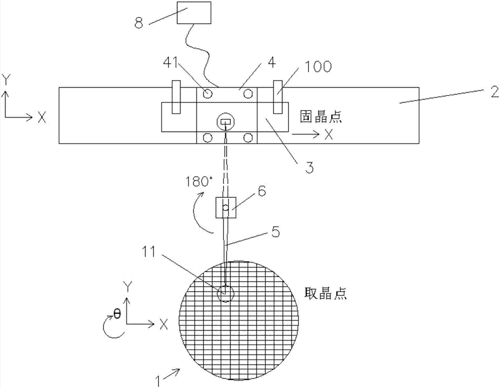
[0026] In order to achieve the purpose of the present invention, as shown in the figure, one embodiment of the present invention is: a crystal extraction and crystal bonding device, including:

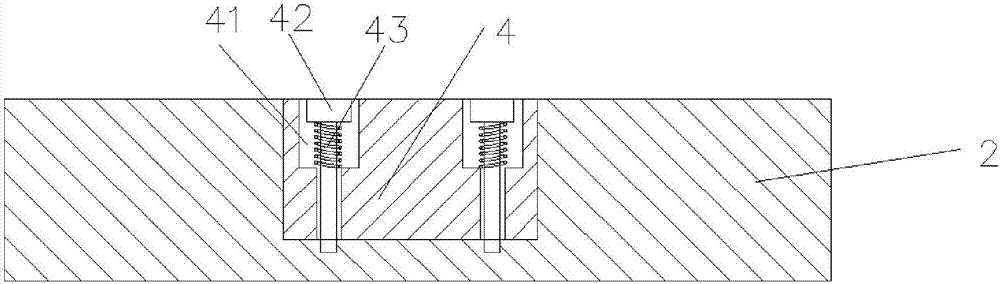
[0027] Solid crystal table 2, solid crystal table 2 moves along X, Y direction, and plane fixture seat 4 is embedded on solid crystal table 2, and plane fixture seat 4 is flush with solid crystal table 2, and plane fixture seat 4 is connected with Heating device 8;

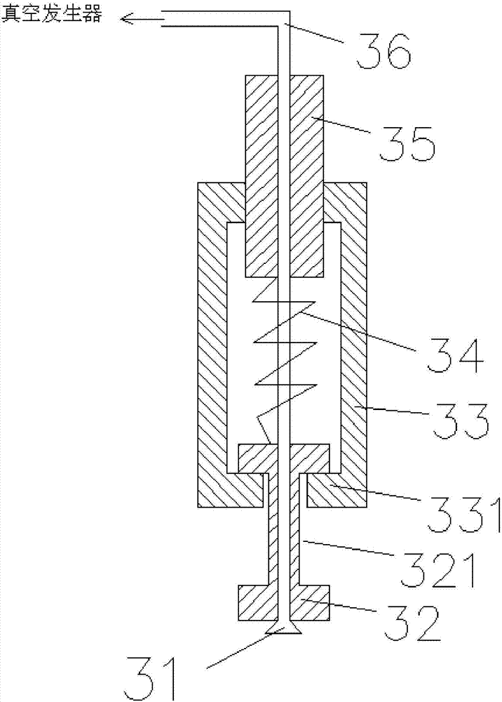
[0028] The rotating arm 5 is provided with a welding head that moves back and forth along the axis of rotation parallel to the rotating arm 5, and the welding head is used for crystal extraction and solid crystal;

[0029] Substrate 3. The substrate 3 is located above the die-bonding table 1 and moves in the X direction relative to the die-bonding table 1. The substrate 3 is fixed by the clamping jaws 100, and the stepping motor drives the clamping jaws to perform the feeding motion.

[0030] The first driving device 6, t...


PUM


Abstract

The invention discloses a die taking and die bonding device. A die bonding table moves along an X direction and a Y direction, a planar jig seat is embedded onto the die bonding table and is flush with the die bonding table, a heating device is connected with the planar jig seat, a rotation arm is provided with a welding head, the welding head is used for die taking and die bonding, a substrate is arranged above the die bonding table and does feeding motion relative to the die bonding table along the X direction, a first driving device is used for driving the rotation arm to do circumferential rotation, a wafer table is used for fixing a wafer, and a wafer table driving device is used for driving the wafer table to move along the X direction and the Y direction and driving the wafer table to rotate around a rotation shaft. The die taking and die bonding device has the beneficial effects that the planar jig seat is arranged, the substrate is heated within a certain range, the temperature is stably controlled, and a hole phenomenon is difficult to generate during chip assembly; and during die bonding, a force between the welding head and the substrate is concentrated on the planar jig seat, the requirement on integral smoothness of the die bonding table is greatly reduced, the parallelism of the welding head and the substrate arranged at a chip assembly position is improved, and the surface-mount smoothness of a semiconductor device is ensured.

Description

technical field [0001] The invention relates to the field of crystal-bonding machines, in particular to a crystal-taking and crystal-bonding device and a crystal-bonding machine using the same. Background technique [0002] Die bonding is an extremely important link in the packaging process of semiconductor devices such as ICs. The process of die bonding is as follows: first, the dispensing mechanism (also known as the dispensing module) dispenses glue on the die bonding station of the substrate, and then the semiconductor chip is removed from the wafer by the die bonding swing arm of the die bonding mechanism, and then transferred Go to the crystal bonding station where the glue has been dispensed. Under the same die-bonding yield (quality) conditions, the die-bonding efficiency of the die-bonding machine is an important indicator for evaluating the performance of the die-bonding machine. [0003] For chips with a DAF film on the back, the package size is the same as the ...

Claims


Application Information

Patent Timeline
IPC IPC(8): H01L21/67
CPCH01L21/67144Y02P70/50
Inventor 王敕戴泳雄
Owner SUZHOU ACCURACY ASSEMBLY AUTOMATION CO LTD
Why Eureka
Try Eureka