Pixel structure and liquid crystal display panel

A technology of pixel structure and substrate substrate, applied in nonlinear optics, instruments, optics, etc., can solve the problems of light leakage of the gate line of the curved liquid crystal display, affecting the pixel charging rate, etc., to improve display performance, voltage stability, The effect of increasing the aperture ratio

Inactive Publication Date: 2017-10-20
TCL CHINA STAR OPTOELECTRONICS TECH CO LTD
View PDF6 Cites 3 Cited by
  • Summary
  • Abstract
  • Description
  • Claims
  • Application Information

AI Technical Summary

Problems solved by technology

[0006] The technical problem to be solved by the present invention is that the light-shielding electrode provided on the gate line of the existing pixel structure increases the parasitic capacitance of the gate line, so that the RC delay phenomenon generated on

Method used


Image

  • Pixel structure and liquid crystal display panel
  • Pixel structure and liquid crystal display panel
  • Pixel structure and liquid crystal display panel

Examples


Embodiment 1

[0037] In order to solve the above-mentioned technical problems existing in the prior art, an embodiment of the present invention provides a pixel structure.

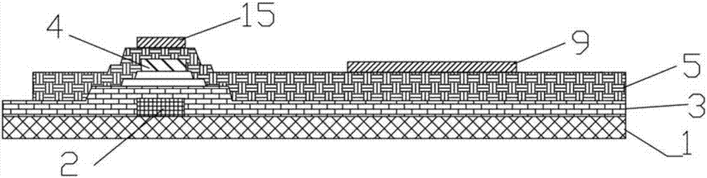
[0038] figure 1 A schematic cross-sectional structure diagram of a pixel structure according to Embodiment 1 of the present invention is shown. figure 2 show figure 1 A top view of the pixel structure shown in .

[0039] refer to figure 1 and figure 2 The pixel structure of this embodiment includes a base substrate 1 , a first metal layer 2 , a first insulating layer 3 , a transparent electrode layer, a second metal layer 4 and a second insulating layer 5 .

[0040] Specifically, the first metal layer 2 is formed on the base substrate 1 , and the first metal layer 2 includes a pattern of gate lines 13 . The first insulating layer 3 is formed on the first metal layer 2 . The second metal layer 4 is formed on the first insulating layer 3 . The second metal layer 4 includes a pattern of data lines 14 . The second...

Embodiment 2

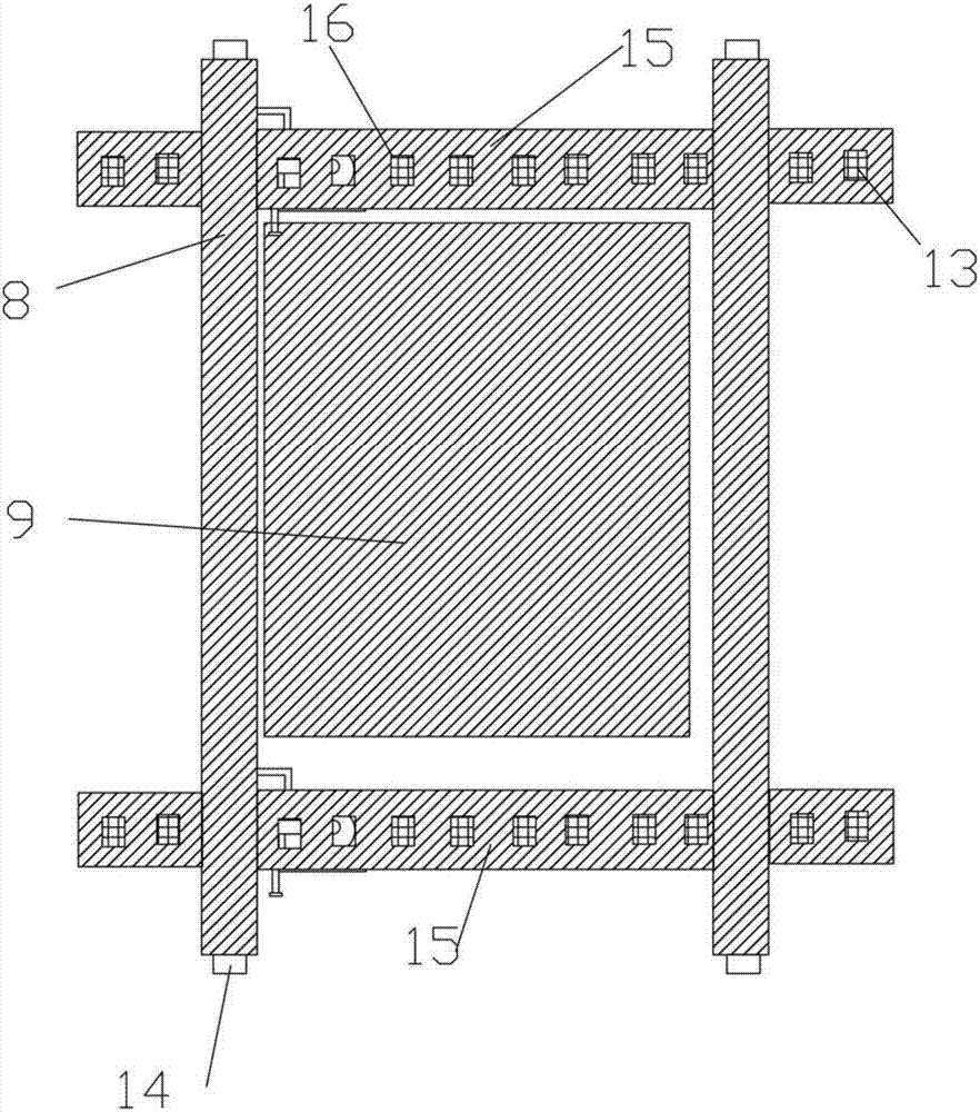
[0046] Correspondingly, image 3 A top view of a pixel structure according to a second embodiment of the present invention is shown. refer to image 3 In this embodiment, on the basis of the first embodiment, the structures of the color-resist layer 6 , the third insulating layer 7 and the transparent electrode layer of the pixel structure are limited.

[0047] Specifically, the color resist layer 6 is formed on the second insulating layer 5 to function as a light filter. The third insulating layer 7 is formed between the color resist layer 6 and the transparent electrode layer, and is used to insulate the color resist layer 6 from the transparent electrode layer. Meanwhile, the transparent electrode layer also includes the pattern of the second transparent electrode 8 , the projection of the second transparent electrode 8 on the second metal layer 4 covers the data line 14 , and the pixel electrode 9 is insulated from the second transparent electrode 8 .

[0048] Therefore...

Embodiment 3

[0055] Correspondingly, Figure 4 A schematic structural diagram of a liquid crystal display screen having the pixel structure of the first embodiment is shown.

[0056] refer to Figure 4 , the liquid crystal display in this embodiment is a liquid crystal display in PSVA mode, and the liquid crystal display is a curved liquid crystal display. The liquid crystal display screen includes a plurality of pixel structures in the first embodiment above.

[0057] The pixel structure of the liquid crystal display of the present invention further includes a liquid crystal layer 10 , a common electrode layer 11 , a color resist layer 6 and an upper glass substrate 12 .

[0058] An upper glass substrate 12 is formed above the transparent electrode layer, the color resist layer 6 is formed on the lower side of the upper glass substrate 12, a common electrode layer 11 is formed on the lower side of the color resist layer 6, and the liquid crystal layer 10 is arranged between the transpar...


PUM


Abstract

The invention discloses a pixel structure and a liquid crystal display panel. The pixel structure includes a substrate, a first metallic layer, a first insulation layer and a transparent electrode layer; the first metallic layer is formed on the substrate, and includes patterns of gate lines; the first insulation layer is formed on the first metallic layer; the transparent electrode layer is formed on the first insulation layer; the transparent electrode layer includes first transparent electrodes; projections of the first transparent electrodes on the gate lines are positioned in local regions of the gate lines, i.e., parts corresponding to the gate lines, of the first transparent electrodes do not completely cover the gate lines. The liquid crystal display panel is a liquid crystal display screen having the pixel structure. The pixel structure can reduce the RC load of the gate lines, the voltage provided by the gate lines is more stable, and influence on the pixel charging rate is reduced. Influence of high-low potential generated by the powered-on gate lines on the transparent electrodes is reduced, lateral light leakage of the gate lines of the pixel structure is avoided, the aperture opening ratio of pixels is improved, and the display quality of the liquid crystal display screen having the pixel structure is improved.

Description

technical field [0001] The invention relates to the field of display technology, in particular to a pixel structure and a liquid crystal display panel with the pixel structure. Background technique [0002] The PSVA (Polmer Stabilized Vertically Aligned, polymer stabilized vertically aligned liquid crystal) mode liquid crystal display uses a vertical electric field in the vertical direction to drive the liquid crystal molecules vertically arranged on the glass substrate, thereby forming a polymer stabilized and vertically aligned liquid crystal. display screen. The liquid crystal display in this mode is in a black display state when no voltage is applied; after a certain voltage is applied, the liquid crystal molecules of the liquid crystal display fall to the horizontal direction, and the liquid crystal display in this mode is in a white display state. [0003] At present, in order to avoid the side light leakage of the liquid crystal display screen caused by the bending o...

Claims


Application Information

Patent Timeline
IPC IPC(8): G02F1/1343
CPCG02F1/1343
Inventor 张蒙蒙宋乔乔
Owner TCL CHINA STAR OPTOELECTRONICS TECH CO LTD
Why Eureka
Try Eureka