Metal layer of compound semiconductor and preparation method thereof

A metal layer and semiconductor technology, which is applied in semiconductor/solid-state device manufacturing, semiconductor devices, electrical components, etc., can solve problems such as residue on the bottom of the photoresist, metal wire falling off, reliability failure, etc., to avoid peeling off, increase gas Tightness, improve the effect of reliability

Active Publication Date: 2020-05-22
XIAMEN SANAN INTEGRATED CIRCUIT
View PDF3 Cites 0 Cited by
  • Summary
  • Abstract
  • Description
  • Claims
  • Application Information

AI Technical Summary

Problems solved by technology

In the electroplating process, the required thickness of the photoresist is relatively thick, and there will be residues on the bottom of the photoresist during the development process, which is difficult to avoid in the existing process
And this defect will cause an obvious gap at the bottom of the electroplated metal after the electroplating is finished
In the subsequent metal etching, due to the siphon effect, the reaction speed here is faster than other places, resulting in larger gaps, and even metal wires falling off, resulting in reliability failures

Method used


Image

  • Metal layer of compound semiconductor and preparation method thereof
  • Metal layer of compound semiconductor and preparation method thereof
  • Metal layer of compound semiconductor and preparation method thereof

Examples


Embodiment 1

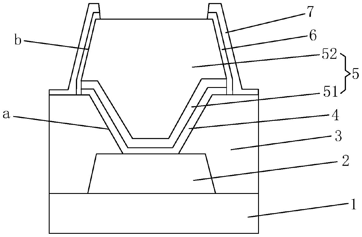
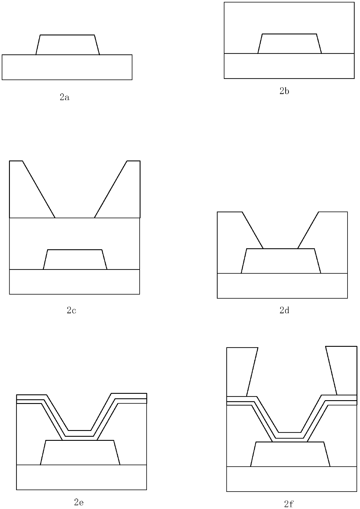
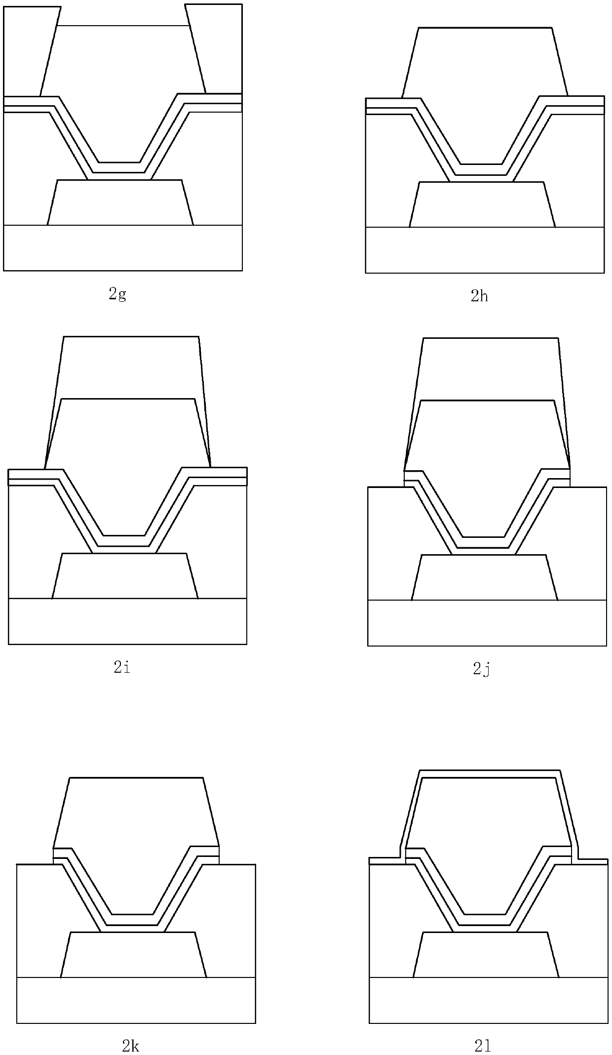
[0034] refer to figure 1 A compound semiconductor metal layer structure includes a first metal layer 2 , an insulating layer 3 , a TiW layer 4 , a second metal layer 5 , a Ti layer 6 and a protective layer 7 disposed on a compound semiconductor wafer 1 . The first metal layer 2 is arranged on the compound semiconductor wafer 1, and the insulating layer 3 covers the first metal layer 2 and the surface of the compound semiconductor wafer 1. The insulating layer 3 is provided with an opening above the first metal layer 2, and the two sides of the opening are directed toward Inward slope 45° to 75°. The TiW layer 4 covers the bottom and sidewalls of the opening 31 and extends to the top surface of the surrounding insulating layer 3 . The second metal layer 5 is formed on the TiW layer 4, fills up the opening and protrudes above the opening, wherein the two sides b of the protruding part are inclined outward by 75° to 85°; the Ti layer 6 covers the TiW layer 4 The sidewall and th...

Embodiment 2

[0058] In Example 1 of figure 2 After the structure of k, repeat figure 2 b to figure 2 The step of k to form the third, fourth and above metal layers on the second metal layer, and then return to figure 2 l step, thereby forming a laminated structure of multiple metal layers.

Embodiment 3

[0060] refer to image 3 , another compound semiconductor metal layer structure, which is different from Embodiment 1 in that it also includes a dielectric layer 8, the dielectric layer 8 covers the first metal layer 2 and the surface of the wafer 1, and the insulating layer 3 is set on the dielectric layer 8. The dielectric layer can be SiN with a thickness of 0.05-0.5 μm, and refer to Example 1 for other structures. This structure is applied to capacitance. Correspondingly, its preparation method is in figure 2 a and figure 2 Add a step between b: deposit an upper dielectric layer on the first metal layer by means of PECVD, and then form an insulating layer.


PUM

PropertyMeasurementUnit
thicknessaaaaaaaaaa
heightaaaaaaaaaa
thicknessaaaaaaaaaa

Abstract

The invention discloses a compound semiconductor metal layer and a manufacturing method thereof. A first metal layer and an insulating layer are arranged on a compound semiconductor wafer successively, an opening is arranged above the first metal layer on the insulating layer, two sides of the opening are inclined inwardly for 45 DEG to 75 DEG, and a TiW layer covers the bottom part and the side wall of the opening and extends to the top surface of the insulating layer around; a second metal layer is formed on the TiW layer and fills the opening and is convex above the opening, and two sides of the convex part are inclined outwardly for 75 DEG to 85 DEG; a Ti layer covers the side wall of the TiW layer and the surface of the second metal layer, and a connection port is opened at the top surface of the second metal layer; and a protection layer covers the Ti layer and the surface of the insulating layer. Through the arrangement of the above structure, the metal layer structure meets technological requirements, the connection stability and the device reliability are improved, the yield of the process and the service life of the product are improved, promotion of an electroplating process in metal layer manufacturing is facilitated, and the cost is reduced.

Description

technical field [0001] The invention relates to a manufacturing process of a semiconductor device, in particular to a metal layer of a compound semiconductor and a preparation method thereof. Background technique [0002] In the III-V compound semiconductors, the metal layer is mainly prepared by evaporation, but the cost of the evaporation process will be relatively high, so the relatively low-cost electroplating metal preparation method will be introduced into the metal layer preparation. Come. In the electroplating process, the required thickness of the photoresist is relatively thick, and there will be residues on the bottom of the photoresist during the development process, which is difficult to avoid in the existing process. And this defect will cause an obvious gap at the bottom of the plated metal after the electroplating is finished. In the subsequent metal etching, due to the siphon effect, the reaction speed here is faster than other places, resulting in larger ...

Claims


Application Information

Patent Timeline
Patent Type & Authority Patents(China)
IPC IPC(8): H01L29/06H01L21/02
CPCH01L21/02505H01L21/02587H01L29/0657
Inventor 王勇
Owner XIAMEN SANAN INTEGRATED CIRCUIT
Why Eureka
Try Eureka