

Masking plate and array substrate manufacturing method
A mask plate and substrate technology, which is applied in semiconductor/solid-state device manufacturing, electrical components, electric solid-state devices, etc., can solve the problems of affecting the quality of substrate packaging, affecting product yield, and poor support effect, so as to save production costs, Reduced substrate mass and friction reduction effects
- Summary
- Abstract
- Description
- Claims
- Application Information
AI Technical Summary
Problems solved by technology
Method used
Image

Examples
Embodiment Construction
[0064] In order to simplify the manufacturing process of the OLED display panel, save the manufacturing cost, and improve the product yield, the embodiment of the present invention provides a method for manufacturing the mask plate and the array substrate. In order to make the purpose, technical solution and advantages of the present invention clearer, the following examples are given to further describe the present invention in detail.
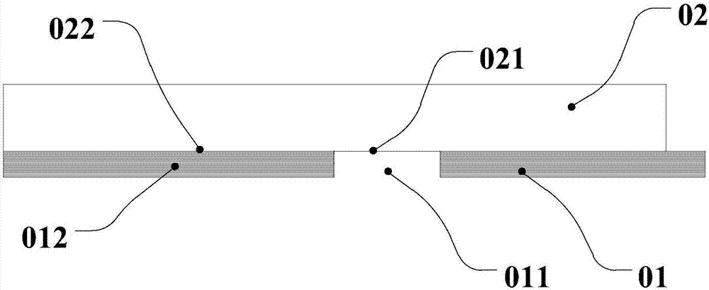
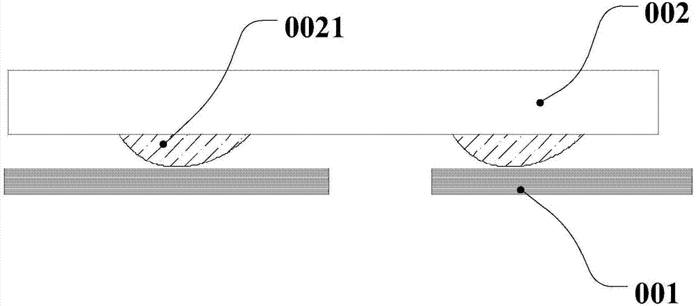
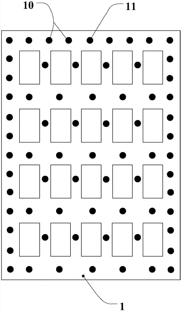
[0065] Such as image 3 with Figure 4As shown, the mask plate provided by the embodiment of the present invention includes a mask plate body 1 and a support structure 10. The mask plate body 1 has a first side surface facing the substrate 2 and a second side surface facing away from the substrate 2 in the evaporation process. On the side surface, the support structure 10 includes a plurality of support protrusions 11 disposed on the first side surface of the mask body 1 , and the surface of the support protrusions 11 is a smooth transition ...
PUM
| Property | Measurement | Unit |
|---|---|---|
| Height | aaaaa | aaaaa |
Abstract
Description
Claims
Application Information