Inductive magnetic sensor for suppressing directional crosstalk and preparation method thereof
A magnetic sensor and inductance technology, applied in the field of inductive magnetic sensor and its preparation, can solve the problems of poor stability and consistency, easy crosstalk, high cost, eliminate cross-sensitivity between axes, improve sensing performance, and suppress inter-axis The effect of crosstalk
- Summary
- Abstract
- Description
- Claims
- Application Information
AI Technical Summary
Problems solved by technology
Method used
Image
Examples
preparation example Construction
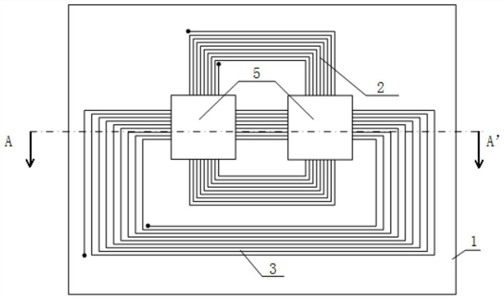
[0018] The preparation method of the inductive magnetic sensor for suppressing directional crosstalk of the present invention includes the following steps: providing an insulating and non-magnetic substrate, fabricating a sensing coil on the insulating and non-magnetic substrate, covering the surface of the sensing coil with an insulating layer, and The bias coil is made on the insulating layer, the bias coil and the sensing coil are partially overlapped, the current direction of the overlapping part of the bias coil and the sensing coil is perpendicular to each other, and the overlapping part of the bias coil and the sensing coil covers another insulating layer , covering the magnetic layer with another insulating layer.
[0019] The present invention provides current to the bias coil, and biases the direction of the non-sensitive axis in the magnetic layer to the insensitive point of the magnetic field, that is, in a neighborhood of the bias magnetic field, the change of the ...
Embodiment 1
[0021] Use silicon dioxide as the substrate, and make the first rectangular planar coil on it by sputtering or electroplating, cover a layer of silicon dioxide film on the first rectangular planar coil, and make the second rectangular planar coil on the film. A planar coil, the second rectangular planar coil partially overlaps with the first rectangular planar coil, and the coil wires in the overlapped part are perpendicular to each other, and a layer of silicon dioxide film is covered on the second rectangular planar coil, and on the silicon dioxide film In the area where the two coils overlap, a layer of FeNi alloy (also can be made of any other magnetically permeable material, such as silicon steel, FeCo alloy) film layer is made by sputtering or electroplating, and the FeNi alloy film layers covering different overlapping areas are not connected. And the minimum distance is greater than the thickness of the film.
Embodiment 2
[0023] In the substrate region of the corresponding position of the FeNi alloy thin film layer in embodiment one, at first make the FeNi alloy thin film layer on it by the method of sputtering or electroplating, on the FeNi alloy thin film layer, make the silicon dioxide thin film layer, with sputtering Or the electroplating method is used to make a rectangular planar coil on it, cover a layer of silicon dioxide film on the coil, and make another rectangular planar coil on the film. The planar coil overlaps with the first rectangular planar coil, and the coil of the overlapping part The wires are perpendicular to each other, and a layer of silicon dioxide film is covered on the second planar coil, and a layer of FeNi alloy film layer is made by sputtering or electroplating in the area where the two coils overlap on the film, covering the FeNi alloy in different overlapping areas. The thin film layers are not connected, and the minimum distance is greater than the thickness of t...
PUM
 Abstract
Description
Claims
Application Information

