

Semiconductor process and semiconductor structure
A semiconductor and process technology, applied in the field of designing semiconductors, can solve problems such as affecting the reliability of chip packaging devices and being easily affected by external forces, so as to avoid adverse effects, avoid damage, and reduce transitional use.
- Summary
- Abstract
- Description
- Claims
- Application Information
AI Technical Summary
Problems solved by technology
Method used
Image

Examples
Embodiment Construction
[0029] Hereinafter, the present invention will be described in more detail with reference to the accompanying drawings. In the various drawings, the same components are denoted by similar reference numerals. For the sake of clarity, various parts in the drawings have not been drawn to scale. Also, some well-known parts may not be shown. For simplicity, the structure obtained after several steps can be described in one figure. In the following, many specific details of the present invention are described, such as the structure, material, size, process and technique of each constituent part, for a clearer understanding of the present invention. However, the invention may be practiced without these specific details, as will be understood by those skilled in the art.
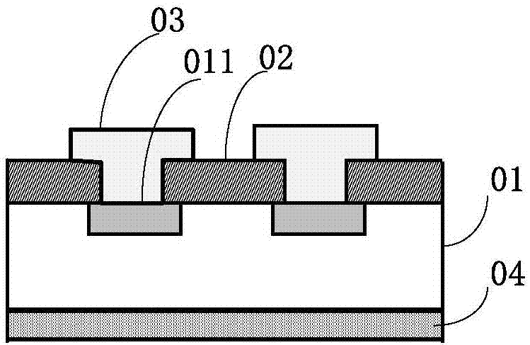
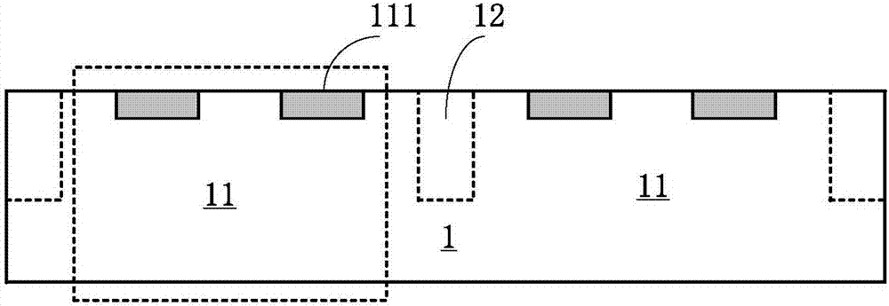
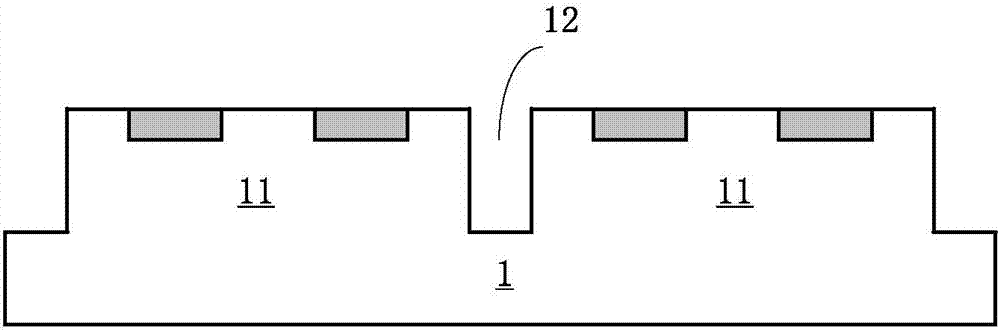
[0030] Figures 2a-2j It is a schematic cross-sectional structure diagram of various process steps of a semiconductor process according to an embodiment of the present invention. The following will combine Fi...
PUM
 Abstract
Description
Claims
Application Information