Trench gate super-junction MOSFET

A technology of trench gate and super junction devices, which is applied in the direction of electrical components, circuits, semiconductor devices, etc., can solve problems such as explosion and failure, and achieve the effect of delaying conduction and improving EAS capability

Active Publication Date: 2017-11-17
SHANGHAI HUAHONG GRACE SEMICON MFG CORP
View PDF3 Cites 7 Cited by
  • Summary
  • Abstract
  • Description
  • Claims
  • Application Information

AI Technical Summary

Problems solved by technology

[0003] In the application of superjunction devices, its single-pulse avalanche breakdown energy (EAS) capability is one of the key performances of the robustness of the device, which is very important. Devices with poor EAS capabilities are often prone to failure in use. In severe cases, even a bombing phenomenon

Method used


Image

  • Trench gate super-junction MOSFET
  • Trench gate super-junction MOSFET
  • Trench gate super-junction MOSFET

Examples


Embodiment Construction

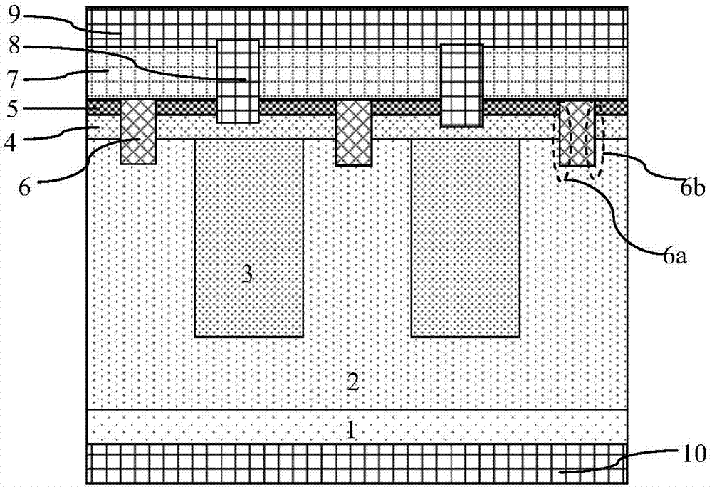
[0029] The technical solution of the embodiment of the present invention is obtained on the basis of analyzing the existing technical problems. Before introducing the technical solution of the embodiment of the present invention in detail, the existing device structure is described as follows, as figure 1 Shown is a schematic structural diagram of an existing trench-gate super-junction MOSFET; the super-junction structure of the existing trench-gate super-junction MOSFET consists of a plurality of N-type pillars 2 and P-type pillars 3 arranged alternately.

[0030] figure 1 Among them, the super junction structure is formed in the N-type epitaxial layer 2, the N-type epitaxial layer 2 is formed on the surface of the semiconductor substrate 1, and a plurality of super junction trenches are formed in the N-type epitaxial layer 2, so The P-type pillar 3 is composed of the P-type semiconductor layer 3 filled in the super junction trench. Usually, the P-type semiconductor layer 3 ...


PUM


Abstract

The invention discloses a trench gate super-junction MOSFET. The trench gates of the device are formed at the tops of interfaces of the P-type columns and the N-type columns of a super-junction structure and span the corresponding interfaces; the trench regions composed of P wells are formed at the tops of the N-type columns; the source regions are formed on the surface of the trench regions; the tops of the trench regions and the source regions are simultaneously connected to the source electrode composed of a right-side metal layer through the same contact holes; the tops of the P-type columns are connected to the source electrode via contact holes; a parasitic transistor consists of a source region, a trench region, and a drift region at the top of each N-type column; and the trench gates are set into a structure spanning the interfaces of the P-type columns and the N-type columns, so that the side parts of the trench gates in the P-type columns form an avalanche current path away from the parasitic transistor when the device reverse avalanche breaks down, and the EAS capability of the device is improved.

Description

technical field [0001] The invention relates to a semiconductor integrated circuit, in particular to a trench gate super junction MOSFET. Background technique [0002] The super-junction MOSFET adopts a new voltage-resistant layer structure, and uses a series of superjunction structures composed of alternately arranged semiconductor P-type thin layers and N-type thin layers to combine P-type thin layers and N-type thin layers at lower voltages in the off state. The N-type thin layer is depleted to achieve mutual compensation of charges, so that the P-type thin layer and N-type thin layer can achieve high breakdown voltage under high doping concentration, thereby obtaining low on-resistance and high reverse breakdown at the same time Voltage (BV), that is, super junction MOSFET is to use PN, that is, P-type thin layer and N-type thin layer charge balance to reduce the surface electric field (Resurf) technology in the body to improve the BV of the device while maintaining a sm...

Claims


Application Information

Patent Timeline
Patent Type & Authority Applications(China)
IPC IPC(8): H01L29/78H01L29/06
CPCH01L29/0634H01L29/7803H01L29/7813
Inventor 李昊
Owner SHANGHAI HUAHONG GRACE SEMICON MFG CORP
Why Eureka
Try Eureka