

Three-dimensional memory electromigration test structure and manufacturing method thereof
A technology for testing structures and manufacturing methods, which is applied in semiconductor/solid-state device testing/measurement, circuits, electrical components, etc., and can solve problems such as test result deviation and test structure damage, achieve fast and accurate positioning, achieve precise positioning, and improve manufacturing. the effect of the success rate
- Summary
- Abstract
- Description
- Claims
- Application Information
AI Technical Summary
Problems solved by technology
Method used
Image

Examples
Embodiment Construction
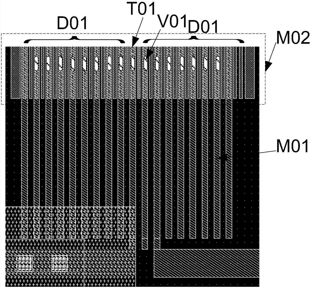
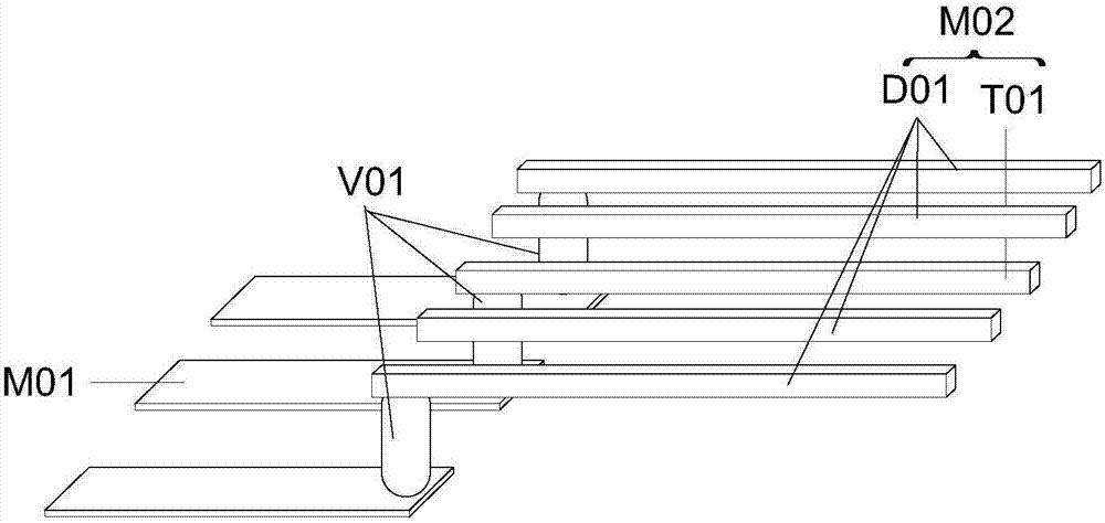
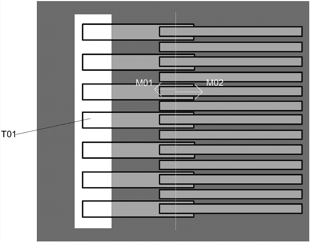
[0046] As mentioned in the background technology section, the positioning method of the test line in the prior art is easy to cause damage to the test structure, which in turn causes deviations in the test results during the test process.
[0047]Specifically, since the main structure of the test line and the virtual line is the same, there is no big difference, so there is no way to locate the test line through the structural difference, and the test line must be located by setting a mark.
[0048] During the sample preparation process of the electromigration test structure, an oxide layer of tens of nanometers to a hundred nanometers must be reserved above the upper metal line M02 to avoid loss of the test line T01 in the M02 during the preparation of the FIB sample. Limited by the observation depth (<200nm) of SEM (Scanning Electron Microscope, scanning electron microscope), the thicker the oxide layer is, the less clear the image will be. Coupled with the fact that the wid...
PUM
 Abstract
Description
Claims
Application Information