Novel carrier enhanced injection IGBT structure

A carrier injection type technology, applied in the direction of electrical components, circuits, semiconductor devices, etc., can solve problems such as improving breakdown voltage

Active Publication Date: 2017-11-21
ZHUZHOU CRRC TIMES SEMICON CO LTD
View PDF4 Cites 0 Cited by
  • Summary
  • Abstract
  • Description
  • Claims
  • Application Information

AI Technical Summary

Problems solved by technology

[0005] The invention provides a novel carrier enhanced injection type IGBT structure to solve the technical problem in the prior art that the breakdown voltage cannot be increased while increasing the current density of the IGBT

Method used


Image

  • Novel carrier enhanced injection IGBT structure
  • Novel carrier enhanced injection IGBT structure
  • Novel carrier enhanced injection IGBT structure

Examples


Embodiment 1

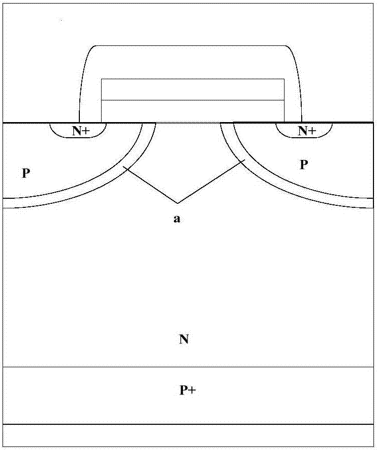
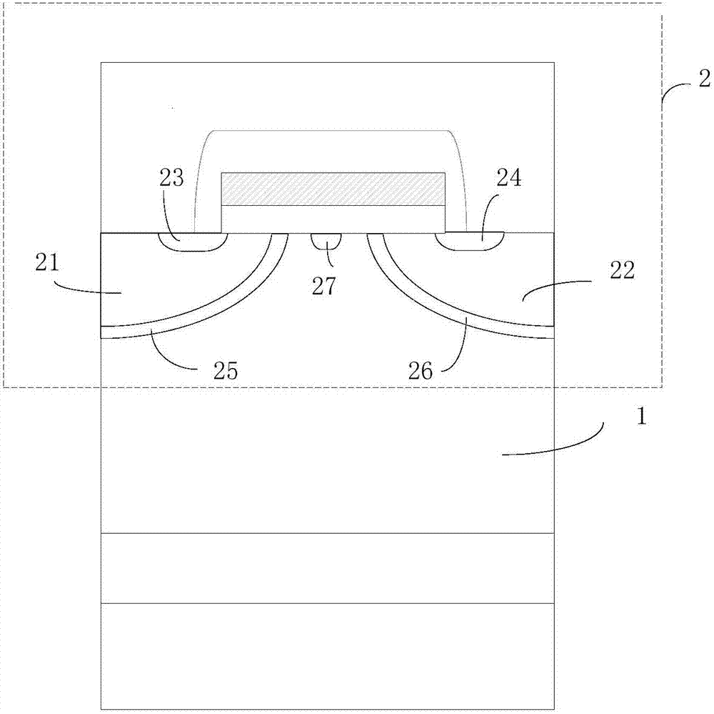
[0024] figure 2 A schematic structural diagram of a novel carrier-enhanced injection IGBT structure provided in Embodiment 1 of the present invention; as figure 2 As shown, this embodiment provides a novel carrier enhanced injection type IGBT structure, including: a semiconductor substrate 1 and a cellular region 2; the cellular region 2 includes a first base region 21 located in the surface of the semiconductor substrate 1, The second base region 22, the first source region 23 located in the first base region 21, the second source region 24 located in the second base region 22, the first carrier storage region 25, the second carrier storage region 26 and the floating region 27 between the first carrier storage region 25 and the second carrier storage region 26, wherein the first carrier storage region 25 connects the first base region 21 and the floating region 27, The semiconductor substrate 1 is separated, and the second carrier storage region 26 separates the second bas...

Embodiment 2

[0030] This embodiment is a supplementary description based on the above embodiments.

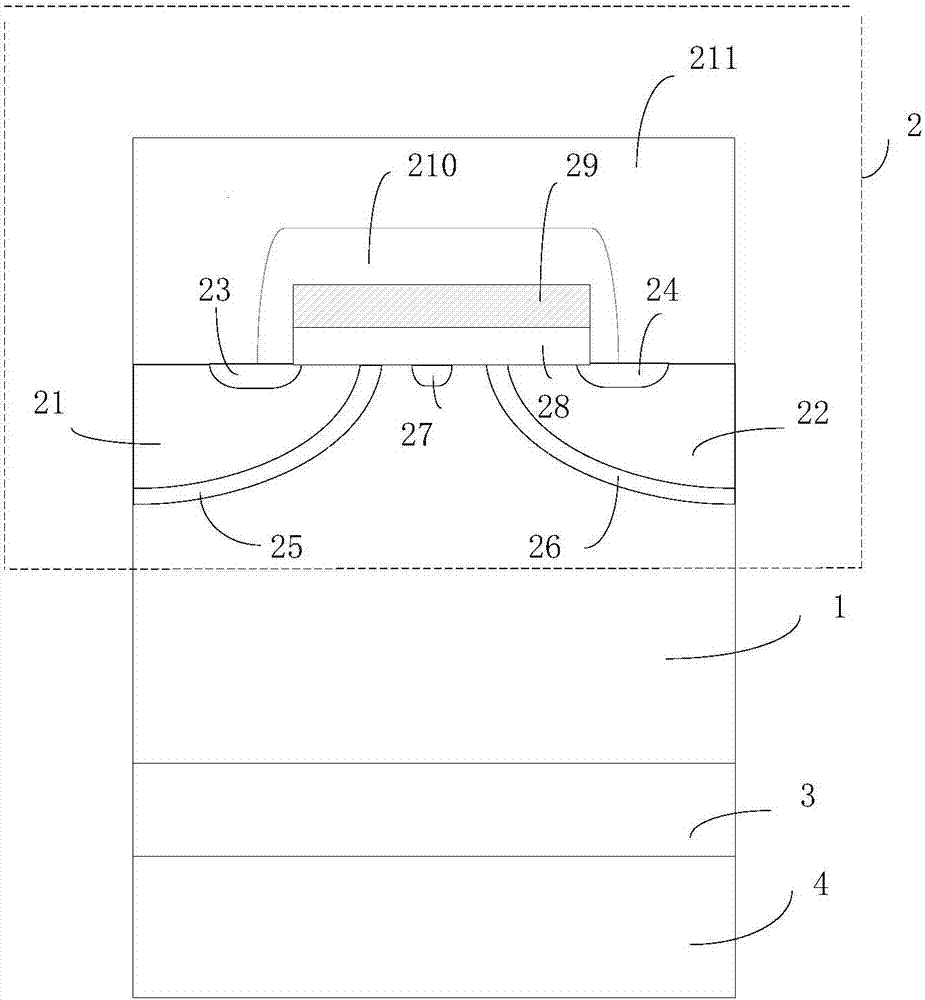
[0031] image 3 A schematic structural diagram of a novel carrier-enhanced injection IGBT structure provided in Embodiment 2 of the present invention; as image 3 As shown, the cell region 2 further includes an oxide layer 28 located on the surface of the semiconductor substrate 1, the oxide layer 28 covers between the first source region 23 and the second source region 24, and covers part of the first source region 23 and the second source region 24. part of the second source region 24 .

[0032] Specifically, the oxide layer 28 covers the region between the first source region 23 and the second source region 24 , and the coverage extends to part of the first source region 23 and part of the second source region 24 .

[0033] Further, the cell region 2 also includes a polysilicon layer 29 covering the oxide layer 28 to form a polysilicon electrode.

[0034] Further, the cell region 2 fu...


PUM


Abstract

The present invention provides a novel carrier enhanced injection IGBT (Insulated Gate Bipolar Transistor) structure. The structure comprises: a semiconductor substrate and a cell region; and the cell region comprises a first base region and a second base region located in the surface of the semiconductor substrate, a first source region located in the first base region, a second source region located in the second base region, a first carrier storage region, a second carrier storage region and a floating region located between the first carrier storage region and the second carrier storage region, wherein the floating region is not contacted with the first carrier storage region and the second first carrier storage region. The arrangement of the floating region allow an ionization accepter formed when the IGBT reverse direction voltage resistance to absorb the part of ionization wires emitted by carrier storage regions located at sides to weaken the curvature effect, reduce the electric field peak value near the cell region and allow the electric field to be uniformly distributed so as to improve the breakdown voltage of the IGBT and improve the purpose of breakdown voltage while improving the IGBT current density.

Description

technical field [0001] The invention relates to the field of semiconductor devices, in particular to a novel carrier enhanced injection type IGBT structure. Background technique [0002] Insulated Gate Bipolar Transistor (IGBT) is a bipolar device controlled by an insulated gate. The higher the non-equilibrium carrier concentration in the body, the more significant the conductance modulation effect and the higher the current density. Taking N-type IGBT with N-type substrate as an example, holes are injected by the anode emitter junction, and electrons are injected by the cathode channel. Affected by the channel resistance, the electron injection capability on the cathode side is limited. In order to enhance the electron injection ability of the IGBT cathode, people introduce the carrier storage layer a, and its structure is shown in the diagram figure 1 shown. The carrier storage layer a enhances the carrier concentration on the cathode side by increasing the N-type injec...

Claims


Application Information

Patent Timeline
Patent Type & Authority Applications(China)
IPC IPC(8): H01L29/06H01L29/739
CPCH01L29/0615H01L29/7393
Inventor 刘国友朱利恒覃荣震罗海辉黄建伟戴小平
Owner ZHUZHOU CRRC TIMES SEMICON CO LTD
Why Eureka
Try Eureka