FinFET device-based unit line non-symmetric storage unit

A technology of storage unit and unit line, which is applied in the direction of information storage, static memory, digital memory information, etc., can solve the problems of small data value, small noise margin, and large delay, so as to reduce dynamic power consumption loss and improve Noise margin, effect of reducing circuit power consumption

Active Publication Date: 2017-11-24
NINGBO UNIV
View PDF3 Cites 4 Cited by
  • Summary
  • Abstract
  • Description
  • Claims
  • Application Information

AI Technical Summary

Problems solved by technology

During the write operation of the memory cell (writing "1" and "0"), the FinFET tube M4 and the FinFET tube M6 will divide the write voltage, so that the written data value is smaller and the noise margin is smaller. As a result, the result of the stored value written to the output terminal Q and the inverting output terminal Qb is unstable, and the circuit function is unstable; and the pull-down network formed by the FINFET tube M3 and the FINFET tube M4 has a problem when the storage unit is in a holding state. There are two leakage current paths, so the leakage current is large, resulting in large leakage power consumption and large delay, which is not conducive to fast and stable data access

Method used


Image

  • FinFET device-based unit line non-symmetric storage unit
  • FinFET device-based unit line non-symmetric storage unit
  • FinFET device-based unit line non-symmetric storage unit

Examples


Embodiment 1

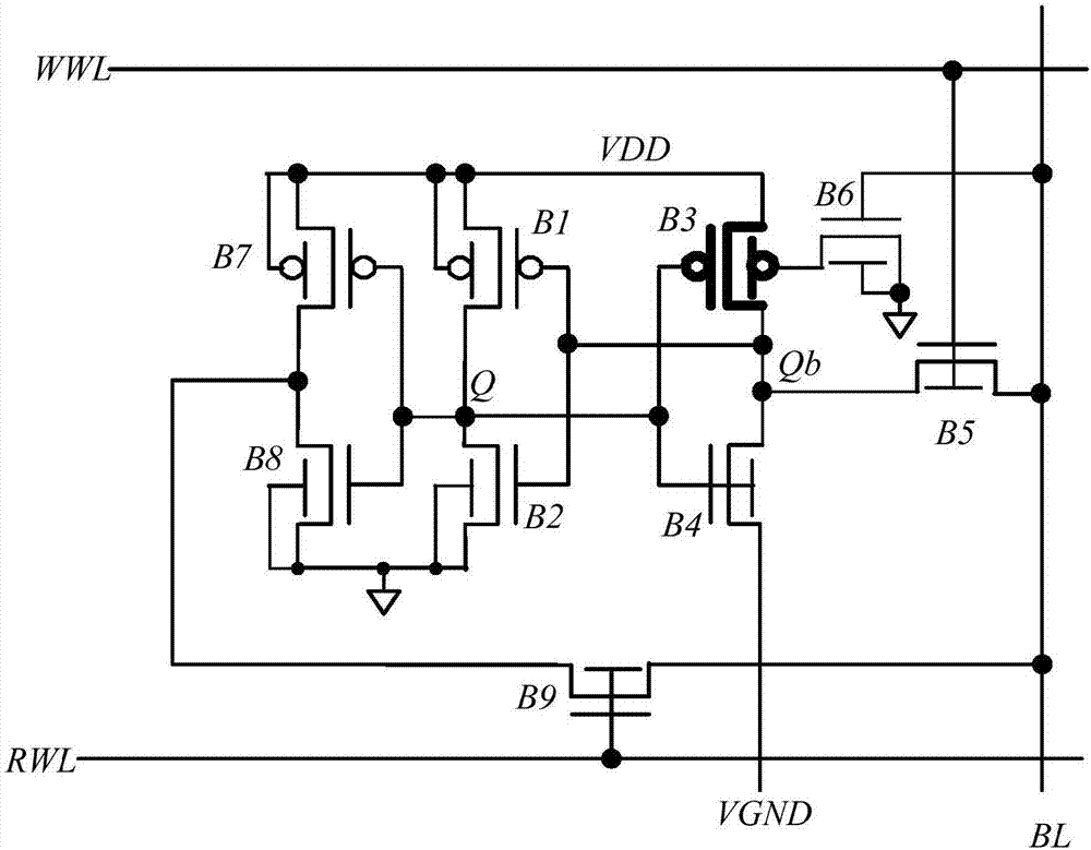
[0016] Embodiment one: if figure 2 As shown, a unit line asymmetric memory cell based on a FinFET device includes a bit line BL, a write word line WWL, a read word line RWL, a first FinFET tube B1, a second FinFET tube B2, a third FinFET tube B3, a fourth FinFET tube FinFET tube B4, fifth FinFET tube B5, sixth FinFET tube B6, seventh FinFET tube B7, eighth FinFET tube B8, and ninth FinFET tube B9; the first FinFET tube B1 and the seventh FinFET tube B7 are respectively low-threshold The P-type FinFET tubes, the second FinFET tube B2, the fourth FinFET tube B4, the fifth FinFET tube B5, the sixth FinFET tube B6, the eighth FinFET tube B8, and the ninth FinFET tube B9 are N-type FinFET tubes with low thresholds, The third FinFET B3 is a high-threshold P-type FinFET; the source of the first FinFET B1, the back gate of the first FinFET B1, the source of the third FinFET B3, the source of the seventh FinFET B7 and The back gate of the seventh FinFET tube B7 is connected and its c...

Embodiment 2

[0017] Embodiment two: if figure 2 As shown, a unit line asymmetric memory cell based on a FinFET device includes a bit line BL, a write word line WWL, a read word line RWL, a first FinFET tube B1, a second FinFET tube B2, a third FinFET tube B3, a fourth FinFET tube FinFET tube B4, fifth FinFET tube B5, sixth FinFET tube B6, seventh FinFET tube B7, eighth FinFET tube B8, and ninth FinFET tube B9; the first FinFET tube B1 and the seventh FinFET tube B7 are respectively low-threshold The P-type FinFET tubes, the second FinFET tube B2, the fourth FinFET tube B4, the fifth FinFET tube B5, the sixth FinFET tube B6, the eighth FinFET tube B8, and the ninth FinFET tube B9 are N-type FinFET tubes with low thresholds, The third FinFET B3 is a high-threshold P-type FinFET; the source of the first FinFET B1, the back gate of the first FinFET B1, the source of the third FinFET B3, the source of the seventh FinFET B7 and The back gate of the seventh FinFET tube B7 is connected and its c...

Embodiment 3

[0019] Embodiment three: as figure 2 As shown, a unit line asymmetric memory cell based on a FinFET device includes a bit line BL, a write word line WWL, a read word line RWL, a first FinFET tube B1, a second FinFET tube B2, a third FinFET tube B3, a fourth FinFET tube FinFET tube B4, fifth FinFET tube B5, sixth FinFET tube B6, seventh FinFET tube B7, eighth FinFET tube B8, and ninth FinFET tube B9; the first FinFET tube B1 and the seventh FinFET tube B7 are respectively low-threshold The P-type FinFET tubes, the second FinFET tube B2, the fourth FinFET tube B4, the fifth FinFET tube B5, the sixth FinFET tube B6, the eighth FinFET tube B8, and the ninth FinFET tube B9 are N-type FinFET tubes with low thresholds, The third FinFET B3 is a high-threshold P-type FinFET; the source of the first FinFET B1, the back gate of the first FinFET B1, the source of the third FinFET B3, the source of the seventh FinFET B7 and The back gate of the seventh FinFET tube B7 is connected and its...


PUM


Abstract

The invention discloses a FinFET device-based unit line non-symmetric storage unit. The unit comprises a bit line, a write word line, a read word line, a first FinFET, a second FinFET, a third FinFET, a fourth FinFET, a fifth FinFET, a sixth FinFET, a seventh FinFET, an eighth FinFET and a ninth FinFET, wherein the first FinFET and the seventh FinFET are low-threshold P-type FinFETs; the second FinFET, the fourth FinFET, the fifth FinFET, the sixth FinFET, the eighth FinFET and the ninth FinFET are all low-threshold N-type FinFETs; and the third FinFET is a high-threshold P-type FinFET. The unit has the advantages that under the condition of not influencing circuit performance, the delay, the power consumption and a power-delay product are all relatively small, the noise margin during write operation is relatively large, and the circuit function stability is relatively high.

Description

technical field [0001] The invention relates to a storage unit, in particular to a unit line asymmetric storage unit based on a FinFET device. Background technique [0002] As the process size enters the nanometer level, power consumption has become a problem that IC designers have to pay attention to. In most digital systems, memory power consumption accounts for an increasing proportion of total circuit power consumption. Static Random Access Memory (SRAM, Static Random Access Memory) is an important component in memory, so it is of great research significance to design SRAM with high stability and low power consumption. The SRAM is mainly composed of a storage array and other peripheral circuits, and the storage array is composed of a storage unit, which is the core of the SRAM, and the performance of the storage unit directly determines the performance of the SRAM. [0003] As the size of transistors continues to shrink, limited by the short-channel effect and the curr...

Claims


Application Information

Patent Timeline
IPC IPC(8): G11C7/18G11C11/418
Inventor 胡建平杨会山
Owner NINGBO UNIV
Why Eureka
Try Eureka