Current-limiting circuit used for MOS tube and MOS switch device

A current-limiting circuit and MOS tube technology, applied in the field of electronics, can solve the problems of slow response speed, unsatisfactory current sharing effect of transconductance consistency, and increase of MOS tube current.

Active Publication Date: 2017-11-24
YUNNAN POWER GRID CO LTD ELECTRIC POWER RES INST
View PDF13 Cites 2 Cited by
  • Summary
  • Abstract
  • Description
  • Claims
  • Application Information

AI Technical Summary

Problems solved by technology

[0004] However, the low-voltage and high-current MOS tubes connected in parallel with multiple tubes often have unsatisfactory current sharing effects due to the transconductance consistency of the MOS tubes, resulting in an abnormal increase in the current of a certain MOS tube. current limiting protection
Existing current-limiting protection circuits usually use fuses, thermal metal fuses and PPTC self-recovery fuses. However, these types of response speeds are relatively slow, and some of them cannot be self-recovery, so it is difficult to truly protect circuits and devices.

Method used


Image

  • Current-limiting circuit used for MOS tube and MOS switch device
  • Current-limiting circuit used for MOS tube and MOS switch device
  • Current-limiting circuit used for MOS tube and MOS switch device

Examples


Embodiment Construction

[0033] Reference will now be made in detail to the exemplary embodiments, examples of which are illustrated in the accompanying drawings. When the following description refers to the accompanying drawings, the same numerals in different drawings refer to the same or similar elements unless otherwise indicated. The implementations described in the following exemplary examples do not represent all implementations consistent with the present invention. Rather, they are merely examples of apparatuses and methods consistent with aspects of the invention as recited in the appended claims.

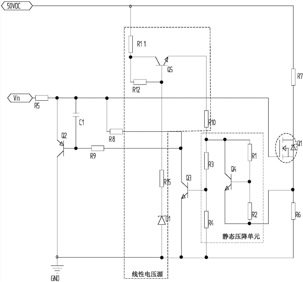
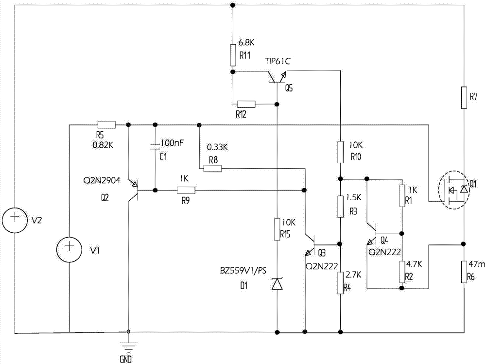
[0034] figure 1 It is a schematic structural diagram of a current limiting circuit for a MOS transistor provided in this application. Such as figure 1 As shown, in addition to the DC voltage source 50VDC in the original switching circuit, the load R7 connected to the DC voltage source 50VDC, and the MOS switch tube Q1 connected to the load R7, the circuit also includes a first PNP transistor Q...


PUM


Abstract

The invention discloses a current-limiting circuit used for an MOS tube and an MOS switch device. The circuit comprises a first PNP type audion, a second NPN type audion, a static voltage drop unit and a current sampling resistor, wherein the emitter of the first PNP type audion is connected with the drive signal source output end of the MOS tube, the base of the first PNP type audion is connected with the collector of the second NPN type audion, and the collector of the first PNP type audion is grounded; the base of the second NPN type audion is connected with one end of the static voltage drop unit, and the emitter of the second NPN type audion is grounded; the other end of the static voltage drop unit is connected with the end, connected with the source of the MOS tube, in the current sampling resistor, and the other end of the current sampling resistor is grounded; the drain of the MOS switch tube is connected with a load, the grid off the MOS switch tube is connected with the drive signal source output end. When the sum of voltage drop generated on the current sampling resistor and voltage of the static voltage drop unit is larger than turn-on voltage of the second NPN type audion, the second NPN type audion is switched on, then the first first PNP type audion is switched on, and G electrode drive voltage of the MOS switch tube is limited to limit currents.

Description

technical field [0001] The present application relates to the field of electronic technology, in particular to a current limiting circuit and a MOS switch device for a MOS tube. Background technique [0002] As we all know, the advantage of MOS tubes is the voltage-driven type semiconductor, which consumes very little current when it is turned on and off, and the on-resistance Rds(on) is quite low, many of which are below 10 milliohms, and some have been achieved below 1 milliohms. Therefore, it is a good solution to choose a MOS tube for switch control. [0003] With the gradual development and progress of the semiconductor industry, the rated operating current of many power MOS tubes can reach 100 amperes, but currently no manufacturer can achieve a rated operating current of 200 A for a single MOS tube. However, in practical applications, a large current of 200A or even 500A often occurs. In this way, a single MOS tube is far from meeting such a large current requirement...

Claims


Application Information

Patent Timeline
Patent Type & Authority Applications(China)
IPC IPC(8): H03K17/082H03K17/687
CPCH03K17/082H03K17/687
Inventor 许守东陈勇李胜男马红升何鑫
Owner YUNNAN POWER GRID CO LTD ELECTRIC POWER RES INST
Why Eureka
Try Eureka