
High-voltage electro-static discharge (ESD) protection circuit

An ESD protection, high-voltage power supply technology, applied in circuits, electrical components, electrical solid devices, etc., can solve problems such as difficult to control latch-up effect, complexity, reliability problems, etc., to eliminate reliability problems, high reliability, and no reliability. Effects of Sexual Problems

Active Publication Date: 2017-11-28
SEMICON MFG INT (SHANGHAI) CORP +1
View PDF8 Cites 2 Cited by
  • Summary
  • Abstract
  • Description
  • Claims
  • Application Information

AI Technical Summary

Problems solved by technology

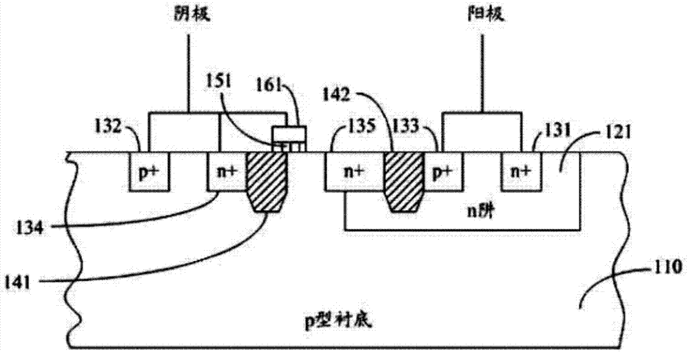
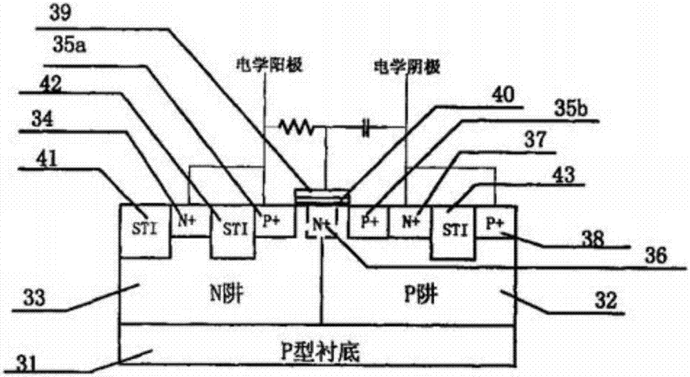
[0004] 1) Although these ESD protection devices have the advantages of small structural area and strong discharge capability, their compatibility and reliability are often difficult to verify due to the use of some parasitic paths and structures;
[0005] 2) The trigger circuit should also be manufactured in an abnormal way, and the reliability of the trigger circuit has yet to be verified
[0006] 3) At the same time, there is also a risk of latch-up that is difficult to control
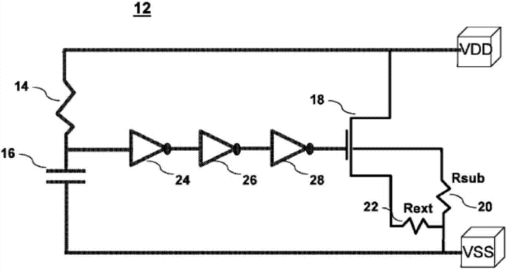
For example, U.S. Patent Application US 8913359B2 discloses an electrostatic discharge protection device (LATCH-UP Free RC-BASED NMOS ESDPOWER-CLAMP IN HV USE) based on RC without latch-up effect, such as Figure 1C As shown, the ESD protection device of this RC structure can discharge the ESD circuit through the RC trigger circuit, but it is still in the BCD process (that is, the bipolar device and the CMOS device are fabricated on the same chip at the same time). There is a reliability problem, because the gate withstand voltage of the LDMOS device of the BCD process can only be 5V, and its inverter structure 24, 26, 28 must withstand the high voltage of VDD during normal operation, otherwise it cannot work , such a requirement can only be used in the general HV process (that is, the high-voltage CMOS manufacturing process), and there is no such device in the BCD process, so it cannot be realized
Another example is the electrostatic discharge protection device (ELECTROSTATIC DISCHARGE PROTECTION FOR HIGH VOLTAGEDOMIANS) disclosed in the US patent application US8830641B2, such as Figure 1D As shown, the whole network stacking structure is used to solve the reliability problem of the HV (high voltage) process. The stacking structure of multiple common devices is mainly used to avoid the withstand voltage problem of the inverter structure, but all the devices are The stacked structure is too complicated. If it is applied to the BCD process, the advantages of LDMOS devices will not be considered, and the implementation area will be relatively large.

Method used


Image

  • High-voltage electro-static discharge (ESD) protection circuit
  • High-voltage electro-static discharge (ESD) protection circuit
  • High-voltage electro-static discharge (ESD) protection circuit

Examples


Embodiment Construction

[0029] In order to make the purpose and features of the present invention more comprehensible, the specific embodiments of the present invention will be further described below with reference to the accompanying drawings. However, the present invention can be implemented in different forms and should not be limited to the described embodiments.

[0030] Please refer to figure 2 The present invention provides a high-voltage ESD protection circuit, which is mainly composed of three parts which are arranged between the high-voltage power line HVDD and the ground line VSS and are sequentially coupled: a bias circuit 201, an ESD trigger circuit 202, and an ESD discharge circuit 203.

[0031] In this embodiment, the bias circuit 201 is used to bias the ESD trigger circuit 202 and provide a bias voltage for it. The bias circuit 201 is mainly composed of four voltage dividing resistors R1, R2, R3, R4 connected in series between the high voltage power line HVDD and the ground line VSS, and ...


PUM


Abstract

The invention provides a high-voltage electro-static discharge (ESD) protection circuit. The high-voltage ESD protection circuit comprises a bias circuit, an ESD trigger circuit and an ESD release circuit which are arranged between a high-voltage power line and a ground line and are sequentially coupled, wherein a plurality of voltage division nodes are arranged on the bias circuit, the ESD trigger circuit mainly comprises a RC delay network in which at least one resistor and a plurality of capacitors are connected, each capacitor is correspondingly coupled to the voltage division node of the bias circuit, and the ESD release circuit is mainly formed by coupling a grid to the RC delay network. The high-voltage ESD protection circuit is simple in structure and high in reliability and can be compatible with a BCD process.

Description

Technical field [0001] The invention relates to the technical field of integrated circuit electrostatic protection, in particular to a high-voltage ESD protection circuit. Background technique [0002] With the development of integrated circuit manufacturing technology, the feature size continues to shrink, making ESD (Electro-static Discharge, electrostatic discharge) more and more impact on integrated circuits. According to statistics, more than one-third of the failures of integrated circuits are caused by ESD. In order to reduce the adverse effects of ESD on integrated circuits and improve the reliability and performance of integrated circuits, the most effective method is to add ESD protection circuits. The ESD protection circuit can convert high-voltage static electricity into transient low-voltage high current, and discharge the current, thereby achieving the purpose of protecting integrated circuits. Therefore, the design of the ESD protection circuit has a relatively hi...

Claims


Application Information

Patent Timeline
Patent Type & Authority Applications(China)
IPC IPC(8): H01L27/02
CPCH01L27/0288
Inventor 王俊卢斌刘森郭之光
Owner SEMICON MFG INT (SHANGHAI) CORP
Learn More