
Manufacturing method and device of electromagnetic shielding part, terminal, computer readable storage medium and electromagnetic shielding part

A technology of electromagnetic shielding and manufacturing method, applied in the field of 3D printing, can solve the problems of structural limitation, affecting the heat dissipation of the chip, heavy weight, etc., to achieve the effect of easy modification, high precision and flexibility, and easy modification

Pending Publication Date: 2017-12-01
大连美光速造科技有限公司
View PDF3 Cites 2 Cited by
  • Summary
  • Abstract
  • Description
  • Claims
  • Application Information

AI Technical Summary

Problems solved by technology

This magnetic field often interferes with external communication Wifi signals, GPS, etc., resulting in communication failure or affecting the internal operation and communication of electrical equipment.
[0003] At present, in order to solve the electric field interference, metal shielding shells and other structures are often used. This structure can solve the interference problem very effectively, but the metal shell seriously affects the heat dissipation of the chip and other outstanding problems. At the same time, the weight is relatively large and the structure is limited.

Method used


Image

  • Manufacturing method and device of electromagnetic shielding part, terminal, computer readable storage medium and electromagnetic shielding part
  • Manufacturing method and device of electromagnetic shielding part, terminal, computer readable storage medium and electromagnetic shielding part
  • Manufacturing method and device of electromagnetic shielding part, terminal, computer readable storage medium and electromagnetic shielding part

Examples


Embodiment 1

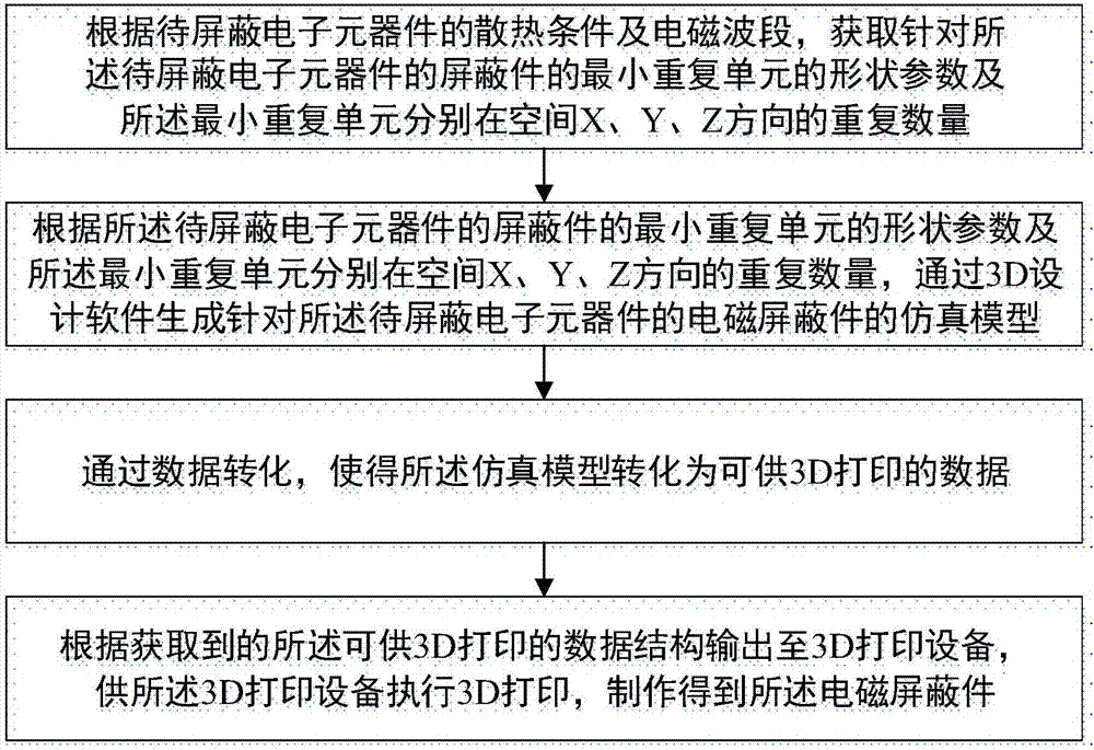
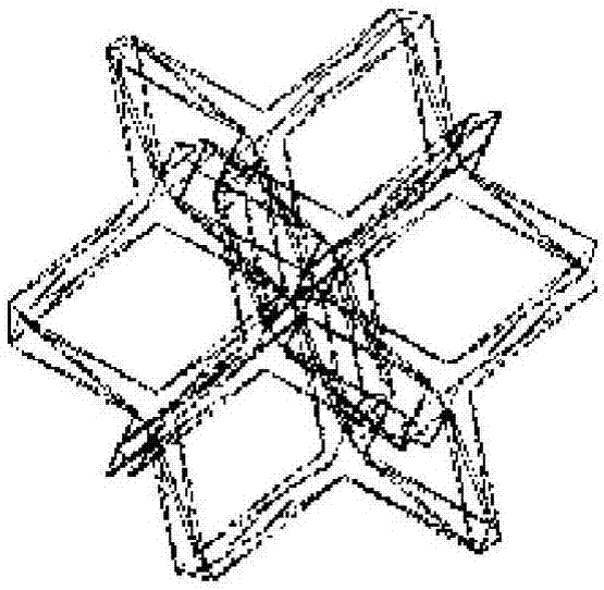
[0054] See attached figure 1 , The manufacturing method of the electromagnetic shield provided by the first embodiment of the present invention includes the following steps:

[0055] Step S1: According to the heat dissipation conditions and the electromagnetic wave band of the electronic components to be shielded, the shape parameters of the smallest repeating unit of the shielding member for the electronic components to be shielded and the number of repetitions of the smallest repeating unit in the X, Y, and Z directions of the space are obtained;

[0056] Step S2: According to the shape parameters of the smallest repeating unit of the shielding part of the electronic component to be shielded and the number of repetitions of the smallest repeating unit in the X, Y, and Z directions of the space, generate electromagnetic shielding for the electronic component to be shielded by 3D design software The simulation model of the piece;

[0057] Step S3: Transform the simulation mod...

Embodiment 2

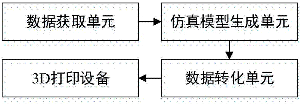
[0067] See attached figure 2 , the manufacturing device of the electromagnetic shielding member provided by Embodiment 2 of the present invention includes:

[0068] The data acquisition unit is used to obtain the shape parameters of the smallest repeating unit of the shielding member of the electronic component to be shielded and the shape parameters of the smallest repeating unit in the X, Y, and Z directions of space, respectively, according to the heat dissipation conditions and the electromagnetic wave band of the electronic component to be shielded. number of repetitions;

[0069] The simulation model generation unit is used to generate the electronic components to be shielded through 3D design software according to the shape parameters of the smallest repeating unit of the shielding part of the electronic component to be shielded and the repetition numbers of the smallest repeating unit in the X, Y, and Z directions of space respectively. The simulation model of the el...

Embodiment 3

[0074] The terminal provided by Embodiment 3 of the present invention includes a processor, a memory, a program for making an electromagnetic shield that is stored in the memory and can run on the processor, and a 3D printing device. The steps of the manufacturing method of the electromagnetic shield provided by the present invention when the production program of the electromagnetic shield is executed by the processor; the 3D printing device is used to perform 3D printing according to the production program of the electromagnetic shield to produce the electromagnetic shield.

[0075] In the process of preparing the electromagnetic shielding part by using the joint application of the terminal and the 3D printing equipment provided by Embodiment 3 of the present invention, firstly, according to the heat dissipation conditions and the electromagnetic wave band of the electronic component to be shielded, the minimum repetition of the shielding part for the electronic component to b...


PUM


Abstract

The invention discloses a manufacturing method and device of an electromagnetic shielding part, a terminal, a computer readable storage medium and the electromagnetic shielding part, and belongs to the field of 3D printing technology application. The method comprises the steps that according to the heat radiation condition and the electromagnetic wave band of a to-be-shielded electronic component, the shape parameter of the minimum repetitive unit of the shielding part for the to-be-shielded electronic component and the repetition quantities, in the X direction, the Y direction and the Z direction of space, of the minimum repetitive unit are obtained; a simulation model of the electromagnetic shielding part for the to-be-shielded electronic component is generated through 3D design software; the simulation model is converted into data capable of being subjected to 3D printing; and 3D printing is executed through 3D printing equipment, and the electromagnetic shielding part is manufactured and obtained. The device can be used for achieving the method. A program used for executing the steps of the method is stored on the terminal. A program used for executing the steps of the method is stored on the computer readable storage medium.

Description

technical field [0001] The present invention relates to the technical field of 3D printing, and in particular to a manufacturing method, device, terminal, computer-readable storage medium and the electromagnetic shielding member based on 3D printing technology. Background technique [0002] With the rapid development of the electronics industry, electronic products and electrical appliances have become indispensable products in industry and life. However, electronic equipment and electrical appliances always produce electromagnetic interference, so that they affect each other. These effects may be quite minor, causing temporary malfunction of the device, or they may cause functional impairment or even damage to the device. The generation of this electromagnetic interference is mainly due to the radiated electric field caused by the constantly changing current, and the change of the electric field produces a changing magnetic field. This magnetic field often interferes with...

Claims


Application Information

Patent Timeline
IPC IPC(8): B29C64/153B29C64/386B22F3/105H05K9/00B33Y10/00B33Y50/00
CPCH05K9/0081B33Y10/00B33Y50/00B22F10/00B22F10/66B22F10/68B22F10/28B22F10/80Y02P10/25
Inventor 李帅薛鹏举李卫东陈志超任申刘亮
Owner 大连美光速造科技有限公司
Learn More