Manufacturing method for junction, manufacturing method for substrate for power module with heat sink, and manufacturing method for heat sink

A manufacturing method and technology for power modules, which are applied in semiconductor/solid-state device manufacturing, manufacturing tools, electrical solid-state devices, etc., can solve the problems of reduced heat dissipation characteristics and increased thermal resistance, and achieve the effect of improving heat dissipation characteristics

Active Publication Date: 2017-12-01
MITSUBISHI MATERIALS CORP
View PDF12 Cites 2 Cited by
  • Summary
  • Abstract
  • Description
  • Claims
  • Application Information

AI Technical Summary

Problems solved by technology

If such a Kirkendall void exists between the power module substrate and the heat sink, there are problems such as an increase in thermal resistance and a decrease in heat dissipation characteristics.

Method used


Image

  • Manufacturing method for junction, manufacturing method for substrate for power module with heat sink, and manufacturing method for heat sink
  • Manufacturing method for junction, manufacturing method for substrate for power module with heat sink, and manufacturing method for heat sink
  • Manufacturing method for junction, manufacturing method for substrate for power module with heat sink, and manufacturing method for heat sink

Examples


no. 1 approach

[0050] Hereinafter, embodiments of the present invention will be described with reference to the drawings.

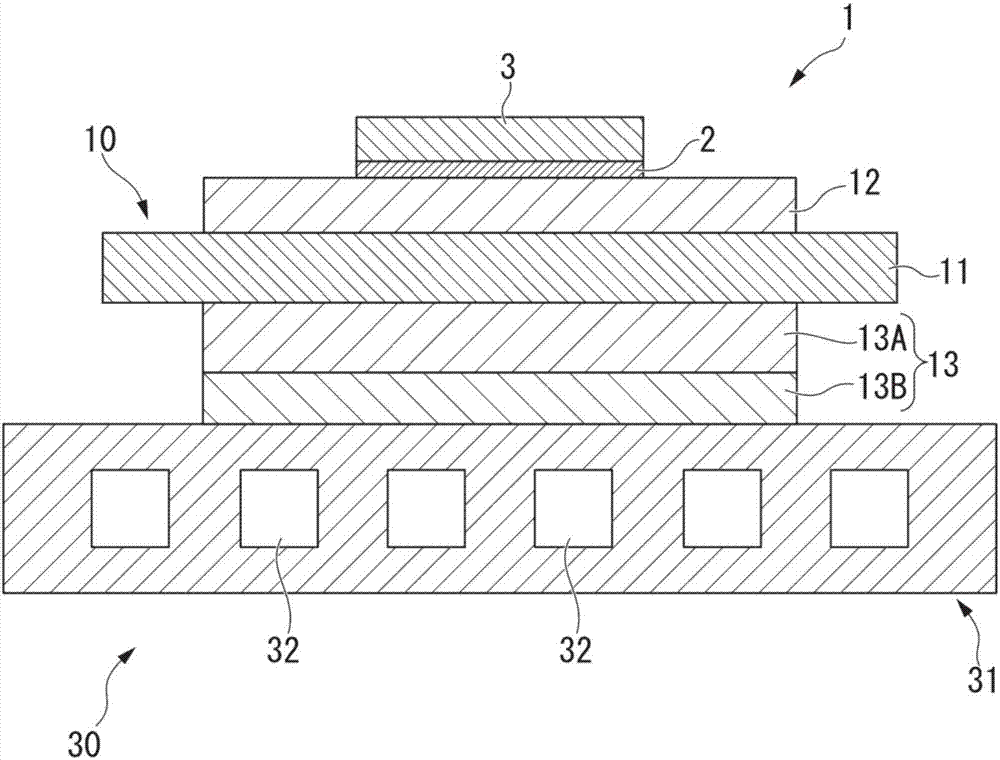
[0051] figure 1 A power module 1 using the power module substrate 30 with a heat sink according to the first embodiment of the present invention is shown in .

[0052] The power module 1 includes a power module substrate 30 with a heat sink and one side of the power module substrate 30 with a heat sink (in the figure 1 The upper surface in the middle) is the semiconductor element 3 bonded by the solder layer 2 .

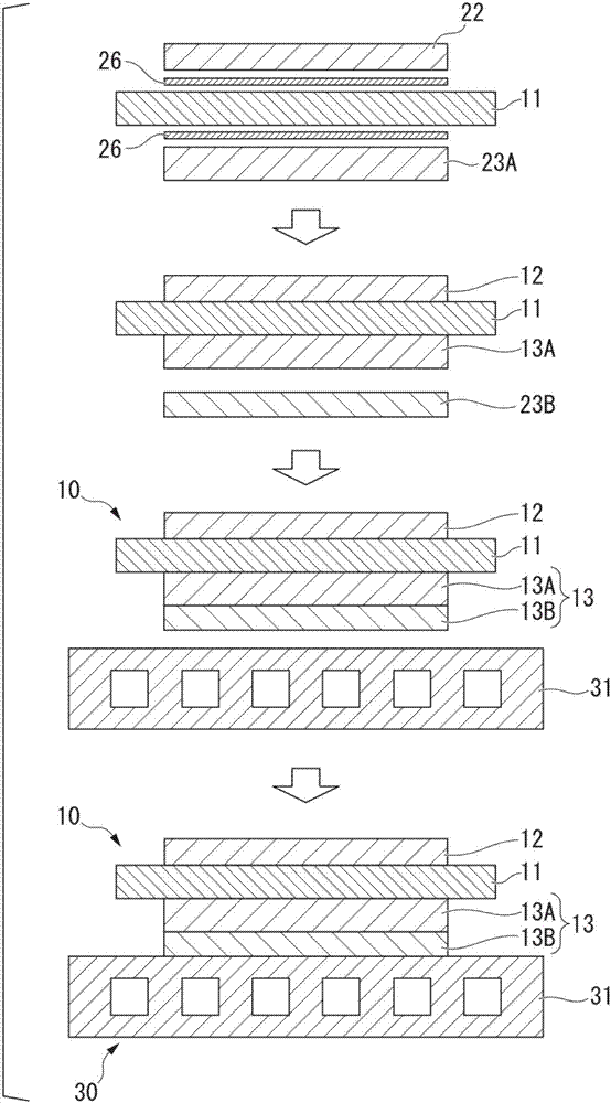
[0053] The power module substrate 30 with heat sink includes the power module substrate 10 and the heat sink 31 bonded to the power module substrate 10 .

[0054] The power module substrate 10 includes a ceramic substrate 11 constituting an insulating layer, and is arranged on one surface of the ceramic substrate 11 (in figure 1 The circuit layer 12 in the center is the upper surface) and the metal layer 13 is arranged on the other surface of the ceramic su...

no. 2 approach

[0100] Next, a heat sink according to a second embodiment of the present invention will be described. Figure 5 A heat sink 101 according to a second embodiment of the present invention is shown in .

[0101] The heat sink 101 has a heat sink main body 110 and one side laminated on the heat sink main body 110 (in the Figure 5 A copper component layer 118 made of copper or a copper alloy. Such as Figure 7 As shown, in the present embodiment, the copper component layer 118 is formed by joining a copper plate 128 made of an oxygen-free copper rolled plate.

[0102] A flow path 111 through which a cooling medium flows is provided in the radiator main body 110 . The heat sink main body 110 is made of an aluminum alloy having a Si concentration in the range of 1% by mass to 25% by mass, specifically ADC3, which is an aluminum alloy for die-casting specified in JIS H 2118:2006. Moreover, this ADC3 is an aluminum alloy containing Si in the range of 9.0-11.0 mass %, and Mg in the...

Embodiment

[0132] Hereinafter, the results of confirmation experiments conducted to confirm the effects of the present invention will be described.


PUM

PropertyMeasurementUnit
diameteraaaaaaaaaa
diameteraaaaaaaaaa
diameteraaaaaaaaaa

Abstract

Provided is a manufacturing method for a junction formed by joining a copper member (13B) comprising copper or a copper alloy, and an aluminum member (31) comprising an aluminum alloy having an Si concentration in a range of not lower than 1 mass% and not higher than 25 mass%. The manufacturing method for the junction is characterized by: setting, in the aluminum member before joining, a circle equivalent diameter D90 of an Si phase in a junction surface with the copper member to be in a range of not smaller than 1 [mu]m and not larger than 8 [mu]m; and joining by solid phase diffusion the aluminum member and the copper member.

Description

technical field [0001] The present invention relates to a method for manufacturing a joined body formed by joining an aluminum part made of an aluminum alloy containing a large amount of Si and a copper part made of copper or a copper alloy, and a power module in which a circuit layer is formed on one side of an insulating layer A method of manufacturing a substrate for a power module with a heat sink in which a heat sink is bonded to the substrate, and a method of manufacturing a heat sink in which a copper component layer is formed on a heat sink main body. [0002] This application claims priority based on Patent Application No. 2015-048151 filed in Japan on March 11, 2015 and Patent Application No. 2016-025164 filed in Japan on February 12, 2016, and the contents thereof are incorporated herein. Background technique [0003] Semiconductor devices such as LEDs and power modules have a structure in which a semiconductor element is bonded to a circuit layer made of a conduc...

Claims


Application Information

Patent Timeline
Patent Type & Authority Applications(China)
IPC IPC(8): B23K20/00B23K1/00H01L23/40B23K101/40
CPCH01L23/473H01L2224/32225C04B37/021C04B37/026C04B2237/121C04B2237/128C04B2237/366C04B2237/402C04B2237/704C04B2237/706C04B2237/708B23K11/20B23K2103/10B23K2103/12B23K2103/18H01L21/4882H01L23/3735H01L23/40B23K20/02H01L21/4846H01L23/49838
Inventor 寺崎伸幸长友义幸
Owner MITSUBISHI MATERIALS CORP
Why Eureka
Try Eureka