Thin film transistor, fabrication method thereof, display substrate and display device

A technology of thin film transistors and substrates, which is applied in the direction of transistors, semiconductor/solid-state device manufacturing, semiconductor devices, etc., can solve the problems of high film quality stress, low light transmittance, substrate warping, etc., and achieve the effect of improving performance

Active Publication Date: 2017-12-12
BOE TECH GRP CO LTD
View PDF6 Cites 3 Cited by
  • Summary
  • Abstract
  • Description
  • Claims
  • Application Information

AI Technical Summary

Problems solved by technology

[0005] Most of the current thin film transistors have problems such as large film quality stress, large capacitive coupling effect, complicated production process and low light transmittance.
In addition, the composite layer structure composed of oxides and nitrides wil

Method used


Image

  • Thin film transistor, fabrication method thereof, display substrate and display device
  • Thin film transistor, fabrication method thereof, display substrate and display device
  • Thin film transistor, fabrication method thereof, display substrate and display device

Examples


Embodiment Construction

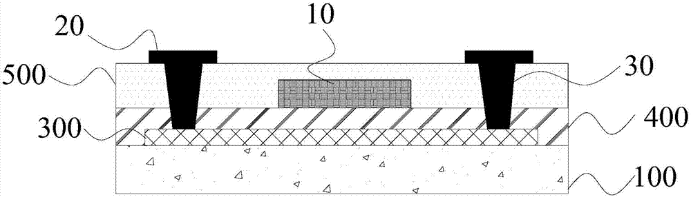
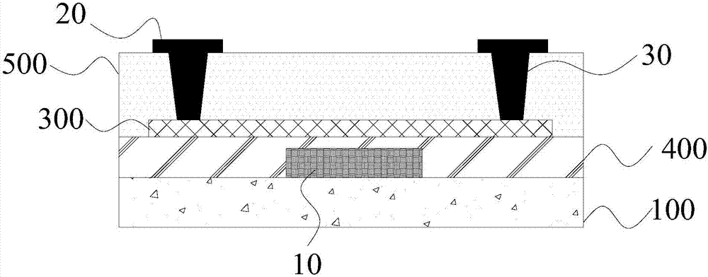
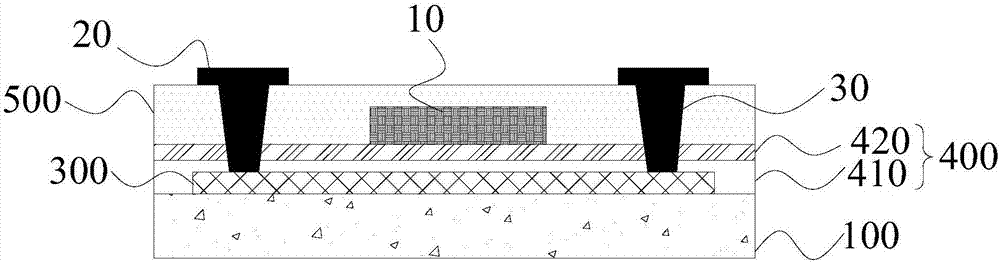
[0026] The following describes in detail the embodiments of the present invention, examples of which are illustrated in the accompanying drawings, wherein the same or similar reference numerals refer to the same or similar elements or elements having the same or similar functions throughout. The embodiments described below with reference to the accompanying drawings are exemplary, only used to explain the present invention, and should not be construed as a limitation of the present invention.

[0027] In the description of the present invention, the orientation or positional relationship indicated by the terms "upper", "lower", etc. is based on the orientation or positional relationship shown in the accompanying drawings, which is only for the convenience of describing the present invention and does not require the present invention to be in a specific manner. The orientation configuration and operation are therefore not to be construed as limitations of the present invention. ...


PUM


Abstract

The invention discloses a thin film transistor, a fabrication method thereof, a display substrate and a display device. The thin film transistor comprises a substrate, an active layer, a grid, a grid insulation layer, an interlayer insulation layer, a source and a drain, wherein the active layer is arranged on the substrate, the grid insulation layer is arranged between the grid and the active layer, the projection of the grid on the active layer is overlapped with at least one part of a channel region of the active layer, the interlayer insulation layer is arranged at one side, far away from the substrate, of the active layer and comprises an organic transparent material, and the source and the drain are arranged at one side, far away the grid insulation layer, of the interlayer insulation layer and are connected with the active layer through a via hole. The thin film transistor has at least one of the following advantages that the membrane stress of the interlayer insulation layer can be reduced, a glass warping phenomenon is improved, the capacitance coupling effect between the source-drain and the grid is reduced, and the light transmittance is effectively improved.

Description

technical field [0001] The present invention relates to the field of display technology, and in particular, to a thin film transistor and a preparation method, a display substrate and a display device. Background technique [0002] At present, liquid crystal displays (LCDs) are widely used in people's daily work and life, such as mobile phones, cameras, computers, televisions, and the like. With the improvement of people's living standards, people's requirements for display quality are also getting higher and higher, which objectively promotes the development of display technology, and new display technologies are also emerging, such as low-temperature polysilicon and organic displays. With the popularization of liquid crystal display devices, users also put forward new requirements for the performance of liquid crystal display devices. [0003] However, the current thin film transistors and their preparation methods, display substrates, and display devices still need to be...

Claims


Application Information

Patent Timeline
IPC IPC(8): H01L29/786H01L21/336
CPCH01L29/66757H01L29/78675
Inventor 詹裕程刘建宏
Owner BOE TECH GRP CO LTD
Why Eureka
Try Eureka