Light emitting diode

A technology of light-emitting diodes and light-emitting surfaces, applied in the field of optoelectronics, can solve the problems of weakening light-emitting efficiency and low light-extraction efficiency, and achieve the effects of reducing lateral propagation, increasing light output, and increasing forward efficiency.

Active Publication Date: 2017-12-19
TIANJIN SANAN OPTOELECTRONICS
View PDF3 Cites 7 Cited by
  • Summary
  • Abstract
  • Description
  • Claims
  • Application Information

AI Technical Summary

Problems solved by technology

[0002] Due to the good lattice matching between AlGaInP material and GaAs substrate, the internal quantum efficiency of high-brightness LEDs grown on it can reach more than 90%, but its light extraction efficiency is very low (only 20%-30%). The means to improve the light extraction efficiency at the end, such as growing DBR layer, coating, roughening, shape design, etc., one of the common methods of DBR reflective layer is used, but the light reflected from the bottom of the reflective layer has to pass through multiple interfaces. Re-reflection will occur at the interface, and the lateral expansion of incident light at a large angle will be enhanced, weakening the light extraction efficiency

Method used


Image

  • Light emitting diode
  • Light emitting diode
  • Light emitting diode

Examples


Embodiment 1

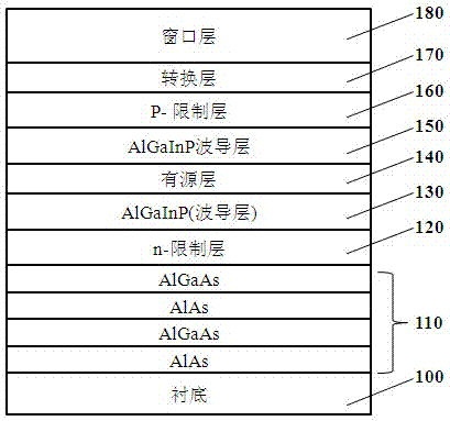
[0051] Please see attached figure 2 The quaternary light-emitting diode of the first preferred embodiment of the present invention may include, from top to bottom: a substrate 100, a combined DBR structure 220, an n-type confinement layer 120, a waveguide layer 130, an active layer 140, waveguide layer 150, p-type confinement layer 160, Al a Ga (1-a) In b P gradient layer 190 , GaP window layer 180 .

[0052] Wherein, the substrate 100 may be a GaAs substrate. The combined DBR structure 220 is composed of N groups of DBR sub-layers, where N≥3 is better, and the preferred value is 3~5. The corresponding wavelength of each DBR sub-layer is adjusted to lengthen the central reflection wavelength to obliquely incident the active area. Light is reflected efficiently. The active layer 140 is a multi-quantum well structure, wherein the barrier layer is Al a1 Ga 1-a1 InP (0.1≤a1≤0.3), the well layer is Al a2 Ga 1-a2 InP, where a1>a2, the materials of the n-type confinement l...

Embodiment 2

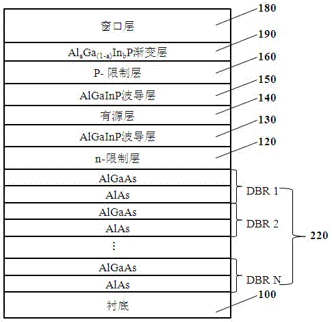
[0064] Please see attached Figure 5 , the quaternary light-emitting diode of the second preferred embodiment of the present invention may include, from top to bottom: a substrate 100, a DBR structure 110, an n-type confinement layer 120, an Al y Ga (1-y) InP graded dielectric waveguide layer 200, waveguide layer 130, active layer 140, waveguide layer 150, Al y Ga (1-y) InP graded dielectric waveguide layer 210, p-type confinement layer 160, Al a Ga (1-a) In b P gradient layer 190 , GaP window layer 180 .

[0065] In this embodiment, conventional materials for the DBR structure 110 , n-type confinement layer 120 , active layer 140 , and p-type confinement layer 160 are selected as required. Form Al y Ga (1-y) InP graded dielectric waveguide layer, Al is formed between the p-type confinement layer and the window layer a Ga (1-a) In b The P graded layer 190 forms a graded refractive index interface so as to reduce the lateral propagation of obliquely incident light an...

Embodiment 3

[0069] Please see attached Figure 6 , the quaternary light-emitting diode of the third preferred embodiment of the present invention may include, from top to bottom: a substrate 100, a combined DBR structure 220, an n-type confinement layer 120, an Al y Ga (1-y) InP graded dielectric waveguide layer 200, waveguide layer 130, active layer 140, waveguide layer 150, Al y Ga (1-y) InP graded dielectric waveguide layer 210, p-type confinement layer 160, Al a Ga (1-a) In b P gradient layer 190 , GaP window layer 180 .

[0070] The combined DBR structure 220 can refer to the method disclosed in Embodiment 1, and set the central reflection wavelength of each DBR sub-layer according to the specific light emission wavelength λ of the active layer and the refraction layer of the material of the DBR layer. al y Ga (1-y) InP graded dielectric waveguide layers 200, 210 and Al a Ga (1-a) In b The P gradient layer 190 can refer to the second embodiment.

[0071] In this embodiment,...


PUM


Abstract

The invention discloses a light emitting diode. By virtue of the light emitting diode, forward effective light output can be increased and / or the inclined incident light can be reflected with the maximum effect through a combined type DBR structure. According to one embodiment of the invention, the light emitting diode comprises a light emitting epitaxial lamination layer which has opposite first surface and second surface and comprises an N type limiting layer, an active layer and a P type limiting layer, wherein the first surface is a light output surface; the combined type DBR structure is arranged on the lower surface of the epitaxial lamination layer, wherein the structure is formed by a combination of N groups of DBR sub layers; and counting from the first pair of DBR sub layers adjacent to the active layer of the N groups of DBR sub layers, the central reflective wavelengths of the DBR sub layers in each layer are <lambda>, <lambda>+<lambda>0, <lambda>+2<lambda>0 until <lambda>+(N-1)*<lambda>0, wherein <lambda> is the light emitting wavelength of the active layer, the (N-1)*<lambda>0 is the maximum blue shift quantity generated by oblique incidence of the active layer, and <lambda>0 is greater than 0.

Description

technical field [0001] The invention belongs to the technical field of optoelectronics, and in particular relates to a light-emitting diode. Background technique [0002] Due to the good lattice matching between AlGaInP material and GaAs substrate, the internal quantum efficiency of high-brightness LEDs grown on it can reach more than 90%, but its light extraction efficiency is very low (only 20%-30%). The means to improve the light extraction efficiency at the end, such as growing DBR layer, coating, roughening, shape design, etc., one of the common methods of DBR reflective layer is used, but the light reflected from the bottom of the reflective layer has to pass through multiple interfaces. Re-reflection will occur at the interface, and the lateral expansion of the incident light at a large angle will be enhanced, which will weaken the light extraction efficiency. [0003] Such as figure 1 It is a conventional AlGaInP LED epitaxial structure, in which there is a large r...

Claims


Application Information

Patent Timeline
Patent Type & Authority Applications(China)
IPC IPC(8): H01L33/04H01L33/32H01L33/10
CPCH01L33/04H01L33/10H01L33/32H01L33/30H01L33/06H01L33/46
Inventor 刘超宁振动王凌飞张军召李维环高文浩吴超瑜王笃祥
Owner TIANJIN SANAN OPTOELECTRONICS
Why Eureka
Try Eureka