Method for detecting channel hole

A detection method and channel technology, which are used in semiconductor/solid-state device testing/measurement, electrical components, circuits, etc., can solve the problems of high cost, difficulty in detection technology, and small radius of channel holes, so as to improve detection efficiency and accuracy. The effect of reducing detection cost and time

Active Publication Date: 2017-12-22
YANGTZE MEMORY TECH CO LTD
View PDF5 Cites 6 Cited by
  • Summary
  • Abstract
  • Description
  • Claims
  • Application Information

AI Technical Summary

Problems solved by technology

[0004] Due to the small radius of the channel hole, the scanning electron microscope cannot accurately display its internal molding, so it is difficult to detect in the detection technology
Sendi

Method used


Image

  • Method for detecting channel hole
  • Method for detecting channel hole
  • Method for detecting channel hole

Examples


Embodiment Construction

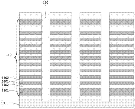
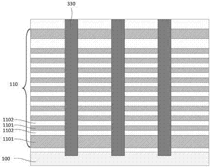
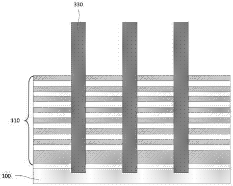
[0029] In order to make the above objects, features and advantages of the present invention more comprehensible, specific implementations of the present invention will be described in detail below in conjunction with the accompanying drawings.

[0030] First of all, in the following description, a lot of specific details are set forth in order to fully understand the present invention, but the present invention can also be implemented in other ways different from those described here, and those skilled in the art can Similar extensions are made below, so the present invention is not limited by the specific embodiments disclosed below.

[0031] Secondly, the present invention is described in detail in combination with schematic diagrams. When describing the embodiments of the present invention in detail, for the convenience of explanation, the cross-sectional view showing the device structure will not be partially enlarged according to the general scale, and the schematic diagra...


PUM


Abstract

The invention discloses a method for detecting a channel hole. The method for detecting a channel hole comprises steps of providing a testing wafer, forming a filling layer in the channel hole, removing part of thicknesses of the stacking layer and the filling layer in order to make the surfaces of the filling layer and the stacking layer leveled in order to obtain a detection layer on the stacking layer and performing measurement of the channel hole on the detection layer. The testing wafer comprises a substrate, the stacking layer on the substrate and the channel hole in the stacking layer; and the stacking layer is obtained through silicon nitride layers and silicon oxide layers which are alternatively stacked. The method for detecting the channel hole can fast and comprehensively detect the formed channel hole, can simultaneously detect multiple holes, can detect the quality of the channel hole in different layers in a three-dimensional way, can accelerate a development progress and can reduce the loss brought by the technical abnormity.

Description

technical field [0001] The invention relates to the field of semiconductors, in particular to a method for detecting channel holes. Background technique [0002] With the continuous advancement of the informatization process, people have more requirements for information storage, and Flash Memory (Flash Memory) storage has emerged as the times require. Flash memory is a long-life non-volatile memory, that is, it can still maintain the stored data information in the case of power failure, and has the advantages of high integration, fast access speed, easy erasing and rewriting, etc. Therefore, it has been widely used. [0003] Three-dimensional (3D) NAND is an emerging type of flash memory with a three-dimensional structure. It solves the limitations of planar (2D) NAND flash memory by vertically stacking multi-layer data storage units and realizes a stacked 3D NAND memory structure. refer to figure 1 , when forming a 3D NAND memory, a stacked layer 110 of a silicon nitrid...

Claims


Application Information

Patent Timeline
IPC IPC(8): H01L21/66
CPCH01L22/12
Inventor 曾最新赵祥辉胡军章诗陈保友
Owner YANGTZE MEMORY TECH CO LTD
Why Eureka
Try Eureka