Rail-to-rail level shift circuit with high linearity

A level shift circuit, high linearity technology, applied in the direction of logic circuit interface device, logic circuit connection/interface layout, etc., can solve problems such as complex circuit design

Active Publication Date: 2017-12-22
UNIV OF ELECTRONICS SCI & TECH OF CHINA
View PDF4 Cites 4 Cited by
  • Summary
  • Abstract
  • Description
  • Claims
  • Application Information

AI Technical Summary

Problems solved by technology

[0004] The purpose of the present invention is to solve the problems existing in the operation of analog signals with high linearity requirements in existing rail-to-rail amplifiers, avoid over-complex circuit design and additional power consumption requirements, and realize high linearity adjustment of external sampling to internal The interface circuit of the common mode level of the op amp

Method used


Image

  • Rail-to-rail level shift circuit with high linearity
  • Rail-to-rail level shift circuit with high linearity
  • Rail-to-rail level shift circuit with high linearity

Examples


Embodiment Construction

[0056] The present invention will be further elaborated below in conjunction with the accompanying drawings and specific embodiments.

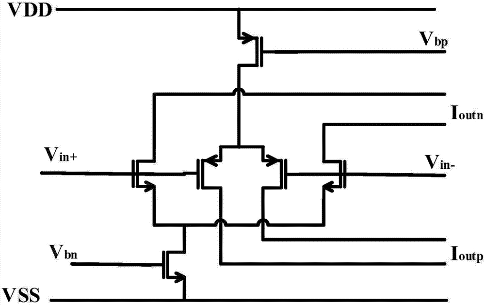
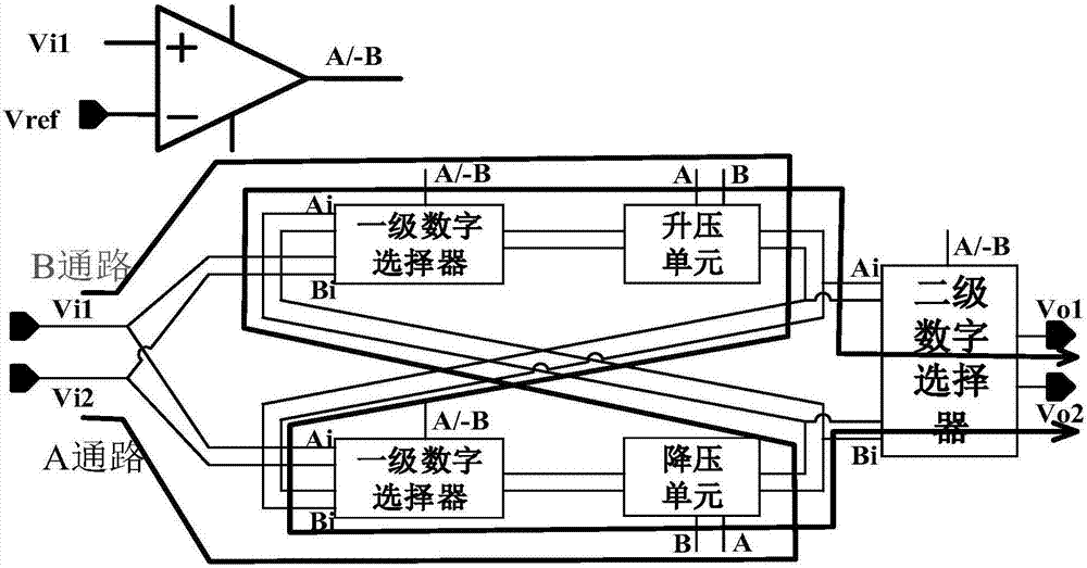
[0057] Compared with the existing rail-to-rail input stage op amp, the level shift circuit provided by the present invention is equivalent to the complementary folded common source stage of the op amp, such as figure 2 Shown is the circuit topology diagram of the present invention, including a first-level digital selector Data Selector I, a step-up unit Level Up, a step-down unit Level Down, a second-level digital selector Data Selector II, and an operation strategy comparator Vin Comparator.

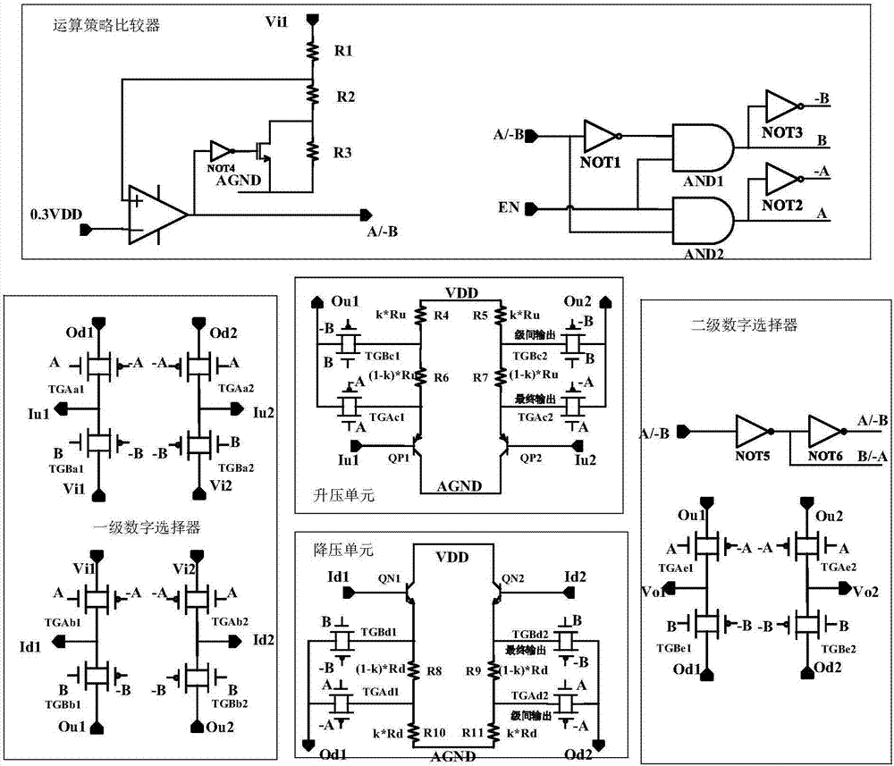
[0058] The computing strategy comparator in this embodiment is such as image 3 As shown, it includes the first resistor R1, the second resistor R2, the third resistor R3, the first inverter NOT1, the second inverter NOT2, the third inverter NOT3, the fourth inverter NOT4, the first and Gate AND1, second AND gate AND2, comparator and NMOS transistor, ...


PUM


Abstract

A rail-to-rail level shift circuit with high linearity belongs to the electronic circuit field. an computing strategy comparator and two-grade digit selectors are employed to generate first A channel control signals A and second A channel control signals -A, or first B channel control signals B and second B channel control signals -B to control input voltage to access an A channel or a B channel, wherein the A channel is formed by allowing input voltage of the level shift circuit to pass through a first-grade digit selector, a voltage reduction unit, the first-grade digit selector, a boosting unit and a second-grade digit selector, and the B channel is formed by allowing the input voltage of the level shift circuit to pass through the first-grade digit selector, the boosting unit, the first-grade digit selector, the voltage reduction unit and the a second-grade digit selector. The complex circuit design and the extra power consumption demand are avoided, and an interface circuit of a common mode level through high linearity regulation of external sampling to an internal operational amplifier.

Description

technical field [0001] The invention belongs to the field of basic electronic circuits, and in particular relates to the design of a rail-to-rail level displacement circuit with high linearity. Background technique [0002] The analog signal collected from the external sampling circuit generally has the characteristics of a wide common-mode range. When the general amplifier processes this analog signal, it cannot be effectively amplified because it exceeds the common-mode input range. The general processing method is to use a rail-to-rail input amplifier structure for signal amplification, that is, to use a combination of NMOS input pair transistors and PMOS input pair transistors, and to select and conduct different pairs of transistors in different common-mode input ranges. Existing typical rail-to-rail input stage circuits such as figure 1 As shown, but the amplification effect of this amplifier will have a large difference when the common-mode input is at the center of ...

Claims


Application Information

Patent Timeline
Patent Type & Authority Applications(China)
IPC IPC(8): H03K19/0175
CPCH03K19/017509
Inventor 周泽坤容浚源石跃张家豪李登维张波
Owner UNIV OF ELECTRONICS SCI & TECH OF CHINA
Why Eureka
Try Eureka