Semiconductor structure and its preparation method

A semiconductor and well region technology, applied in semiconductor/solid-state device manufacturing, semiconductor devices, electrical components, etc., can solve problems such as MOS damage, threshold voltage test failure, short circuit, etc.

Active Publication Date: 2019-11-08
FOUNDER MICROELECTRONICS INT
View PDF5 Cites 0 Cited by
  • Summary
  • Abstract
  • Description
  • Claims
  • Application Information

AI Technical Summary

Problems solved by technology

During the test, the source is grounded at 0V. When the applied voltage of the polycrystalline gate exceeds the breakdown voltage of the thin gate oxide, the gate oxide between the gate and the source (such as figure 2 The thin gate oxide region shown by the dotted circle) will be broken down, resulting in a short circuit between the gate Gate and the source source of the MOS transistor, MOS damage, and threshold voltage test failure

Method used


Image

  • Semiconductor structure and its preparation method
  • Semiconductor structure and its preparation method
  • Semiconductor structure and its preparation method

Examples


Embodiment Construction

[0032] In order to make the purpose, technical solutions and advantages of the embodiments of the present invention clearer, the technical solutions in the embodiments of the present invention will be clearly and completely described below in conjunction with the drawings in the embodiments of the present invention. Obviously, the described embodiments It is a part of embodiments of the present invention, but not all embodiments. Based on the embodiments of the present invention, all other embodiments obtained by persons of ordinary skill in the art without creative efforts fall within the protection scope of the present invention.

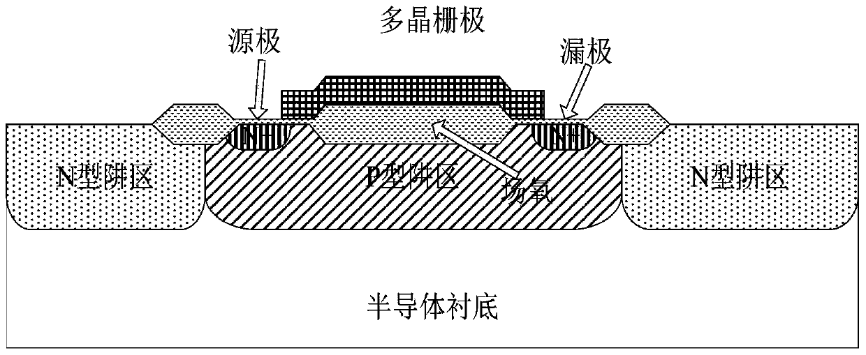
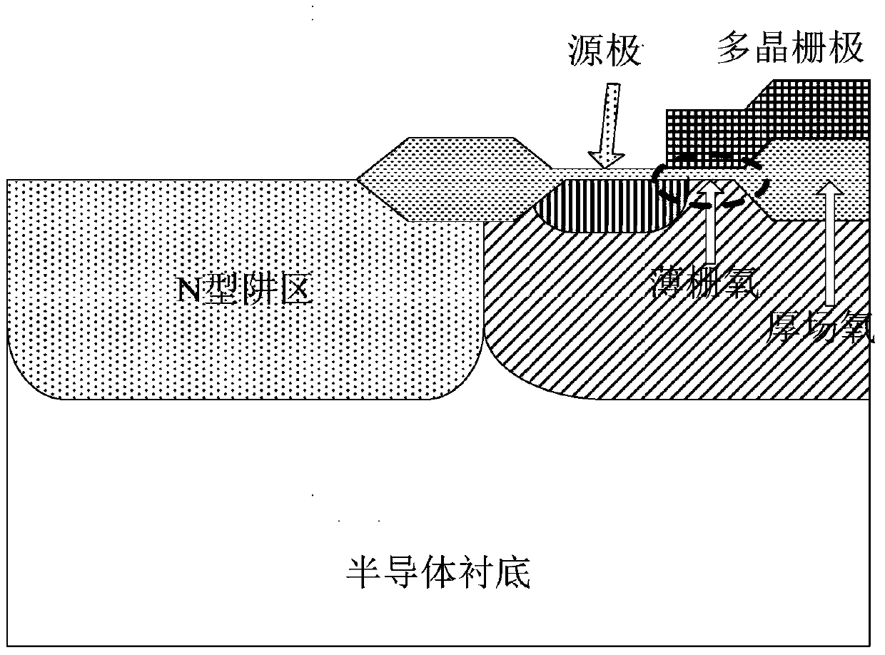
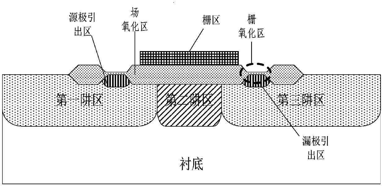
[0033] In order to solve the technical problems mentioned in the background art, the present invention designs a new semiconductor structure, which can be used to test the thick-field oxygen threshold voltage.

[0034] image 3 A schematic structural diagram of the semiconductor structure provided by Embodiment 1 of the present invention is shown...


PUM


Abstract

The invention provides a semiconductor structure and the preparation method thereof. The semiconductor structure comprises a substrate, a first well region having a first doping type formed in the substrate, a second well region having a second doping type and a third well region having a first doping type, wherein the second well region is disposed between the first well region and the third well region; a source lead-out region formed in the first well region, a drain lead-out region formed in the third well region; and a field oxide region and a gate oxide region covering the surface of the substrate and disposed adjacent to each other; wherein the field oxide region is located above the substrate between the source lead-out region and the drain lead-out region, and the thickness of the field oxide region is greater than that of the gate oxide region. The semiconductor structure further comprises a gate region formed on the field oxide region, wherein the gate region completely covers the second well region, and covers only part or all of the field oxide region without covering the gate oxide region. The semiconductor structure provided by the present invention can satisfy the normal measurement of the threshold voltage of the semiconductor structure.

Description

technical field [0001] The invention relates to the technical field of semiconductor chip manufacturing technology, in particular to a semiconductor structure and a preparation method thereof. Background technique [0002] Process Control Monitor (PCM), also known as WAT (wafer acceptance test), is an electrical measurement of the chip after the process is completed, and is used to check whether each process meets the standard. Usually PCM testing includes Vt&BV&Beta testing of various devices, resistance testing of each layer, oxide film capacitance testing, oxide layer withstand voltage testing, PN junction testing between layers, etc. [0003] An existing thick-field oxygen MOS tube has a structure such as figure 1 shown. If a thick-field oxygen MOS transistor with such a structure is used in actual integrated circuit manufacturing, when the threshold voltage test of the MOS transistor is performed, the MOS transistor is often damaged and fails to be tested. [0004] ...

Claims


Application Information

Patent Timeline
Patent Type & Authority Patents(China)
IPC IPC(8): H01L29/78H01L29/423H01L21/336
CPCH01L29/42356H01L29/4238H01L29/66477H01L29/78
Inventor 石金成马万里高振杰李杰英崔永军
Owner FOUNDER MICROELECTRONICS INT
Why Eureka
Try Eureka