Annealing method

A technology of annealing and annealing treatment, applied in electrical components, semiconductor/solid-state device manufacturing, circuits, etc., can solve the problems of uneven heat absorption efficiency, uneven heat distribution, uneven device performance, etc., to improve device performance uniformity and heat distribution. uniform effect

Inactive Publication Date: 2018-01-09
YANGTZE MEMORY TECH CO LTD
View PDF6 Cites 1 Cited by
  • Summary
  • Abstract
  • Description
  • Claims
  • Application Information

AI Technical Summary

Problems solved by technology

[0004] In order to solve the above technical problems, this application provides an annealing method to solve the uneven heat distribution caused by the difference in heat absorption efficiency of substrates with patterned structures due to differences in materials and density of active regions in traditional annealing methods , resulting in the problem of non-uniform device performance

Method used


Image

  • Annealing method
  • Annealing method
  • Annealing method

Examples


Embodiment Construction

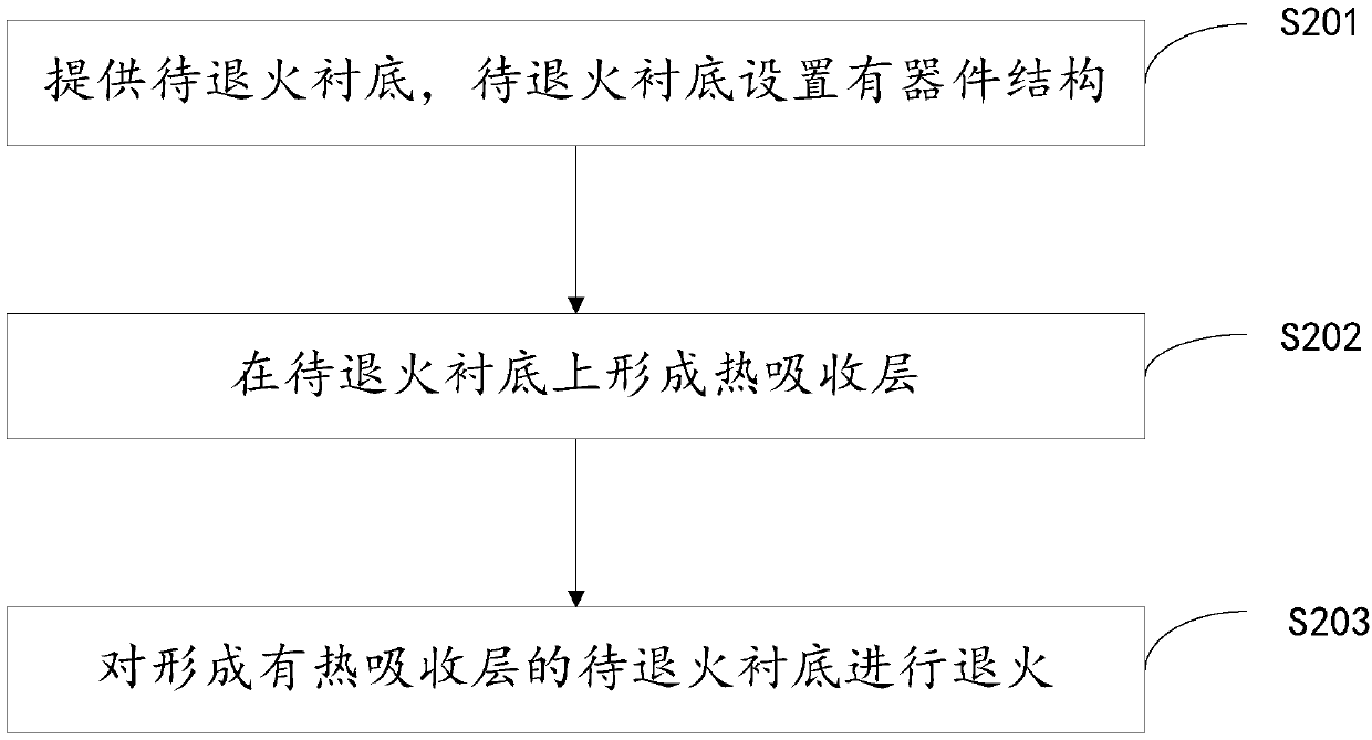
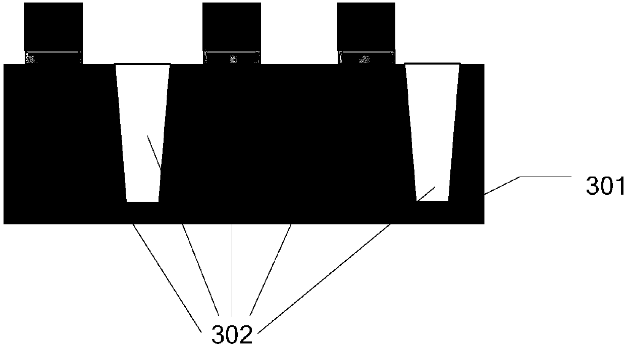
[0029] A semiconductor is a substance whose conductivity is between that of a conductor and an insulator. In order to make semiconductor materials form PN junctions (the material basis of diodes and triodes), resistors, and interconnect lines in semiconductor devices, it is often necessary to change the electrical properties of the materials through doping.

[0030] Doping can be understood as adding the required impurities into the semiconductor material according to the required concentration and distribution. Doping can generally be achieved by diffusion or ion implantation. Generally, thermal diffusion is used for high-concentration deep junction doping, and ion implantation is used for shallow junction high-precision doping. Ion implantation can strictly control the doping amount and distribution, and has the characteristics of low doping temperature, less lateral diffusion, and more dopant elements. It can dope various materials, and the impurity concentration is not li...


PUM


Abstract

An embodiment of the invention discloses an annealing method. The method comprises the following steps of providing a to-be-annealed substrate provided with a device structure, forming a heat absorption layer on the surface of the to-be-annealed substrate and annealing the to-be-annealed substrate with the heat absorption layer. The heat absorption layer is generally formed by the same material, and the thickness is relatively uniform and the surface undulation is smaller, so that the heat absorption layer can uniformly absorb the heat during annealing in the annealing process, and furthermore, the heat absorption layer is in contact with the substrate with the device structure, so that the absorbed heat can be transferred to the substrate covered by the heat absorption layer and providedwith the device structure in a heat conduction manner, and thus the heat distribution on the substrate is more uniform to improve the uniformity of the device.

Description

technical field [0001] This application relates to the field of semiconductors, in particular to an annealing method. Background technique [0002] With the development of semiconductor technology, the feature size of complementary metal oxide semiconductor (CMOS) devices is getting smaller and smaller, and the depth of PN junction is getting shallower. In order to reduce the sheet resistance, the activation of implanted ions can be improved by increasing the annealing temperature. accomplish. However, an increase in temperature will lead to an increase in the diffusion of doping elements, which will affect the ion concentration and the depth of the PN junction, thereby affecting device performance. The millisecond-level annealing process can achieve high activation and minimal diffusion through instantaneous high temperature. [0003] Due to the variety of surface patterns on silicon wafers, it can be roughly divided into dense active areas and sparse active areas. The he...

Claims


Application Information

Patent Timeline
Patent Type & Authority Applications(China)
IPC IPC(8): H01L21/02H01L21/268H01L21/324
Inventor 余德钦周文斌吴娴
Owner YANGTZE MEMORY TECH CO LTD
Why Eureka
Try Eureka