Semiconductor structure and forming method therefor

A semiconductor and isolation structure technology, applied in the field of semiconductor structure and its formation, can solve problems such as adverse effects on the electrical performance of semiconductor devices, and achieve the effect of optimizing electrical performance, reducing oxidation, or avoiding oxidation

Active Publication Date: 2018-01-16
SEMICON MFG INT (SHANGHAI) CORP +1
View PDF6 Cites 0 Cited by
  • Summary
  • Abstract
  • Description
  • Claims
  • Application Information

AI Technical Summary

Problems solved by technology

[0004] However, the formation process of the isolation structure in the prior art is likely to adversely affect the electrical performance of the semiconductor device

Method used


Image

  • Semiconductor structure and forming method therefor
  • Semiconductor structure and forming method therefor
  • Semiconductor structure and forming method therefor

Examples


Embodiment Construction

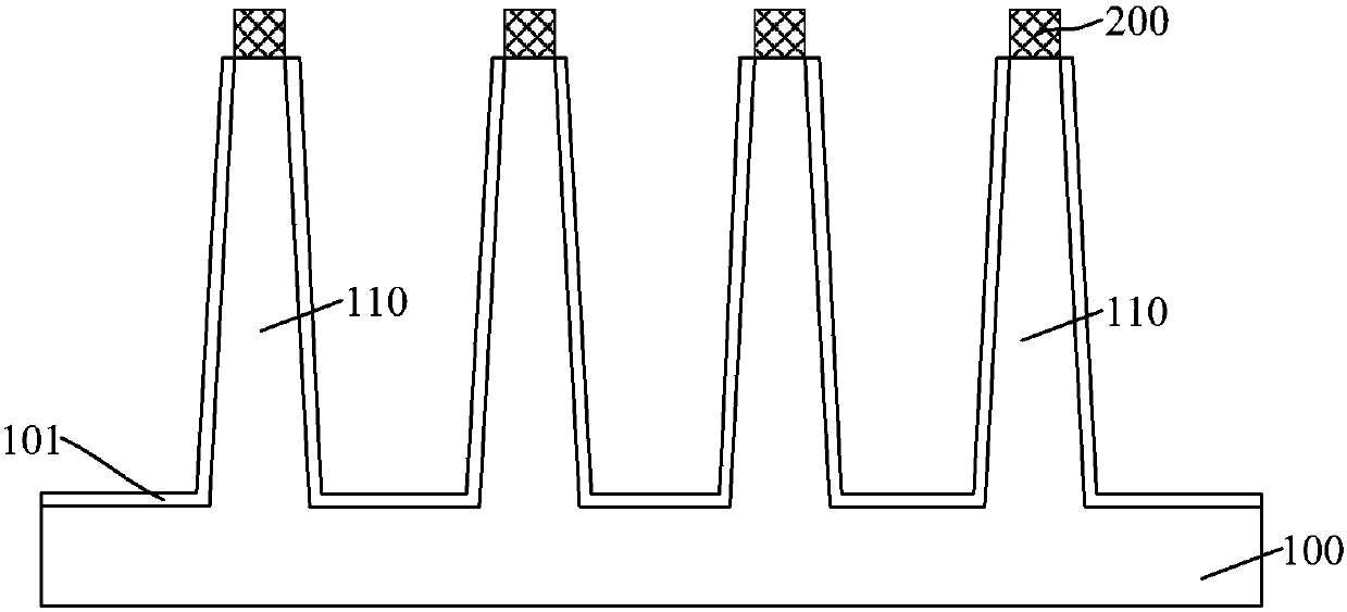
[0029] It can be seen from the background art that the formation process of the isolation structure in the prior art has a bad influence on the electrical performance of the semiconductor device. Analyze the reasons for this:

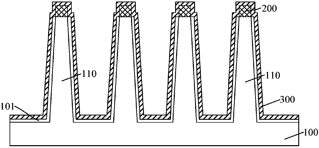
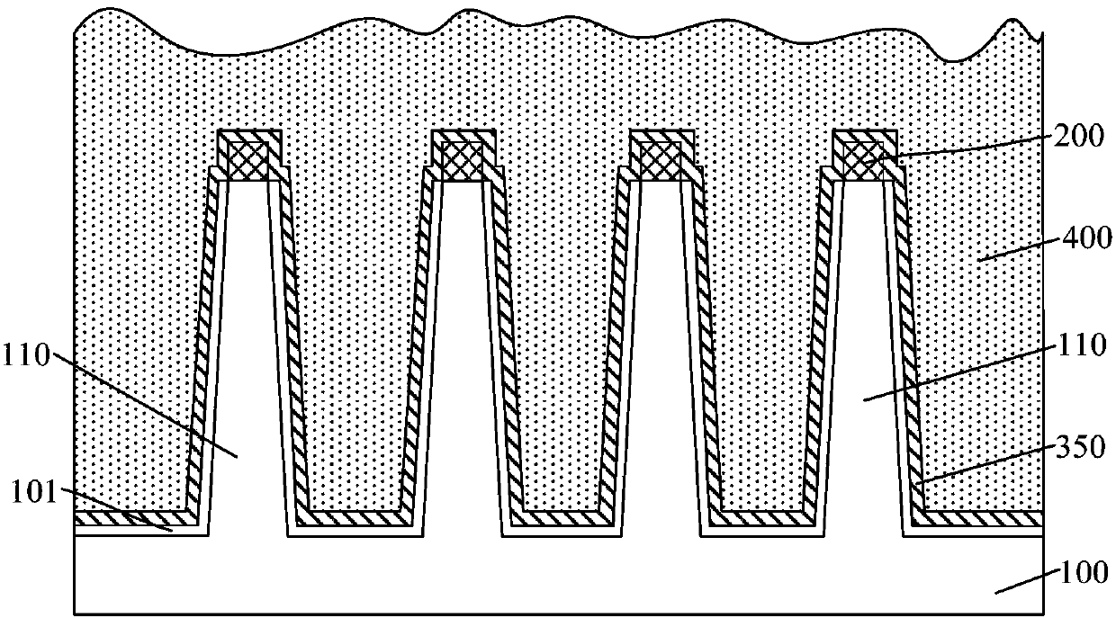
[0030] The process steps of forming the isolation structure mainly include: forming a substrate and fins protruding from the substrate; forming a precursor isolation film on the substrate between adjacent fins; performing an annealing process on the precursor isolation film , converting the precursor isolation film into an isolation film; removing part of the thickness of the isolation film to form an isolation structure.

[0031] However, the process of forming the precursor isolation film may easily oxidize the fin, thereby consuming part of the material of the fin, affecting the size of the fin, and easily leading to a decrease in the electrical performance of the semiconductor device.

[0032] In order to solve the technical problem, the present in...


PUM


Abstract

The invention discloses a semiconductor structure and a forming method therefor, and the method comprises the steps: providing a base which comprises a substrate part and fins bulged from the substrate; forming sacrificial layers on side walls of the fins and at the tops of the fins; forming a precursor isolating membrane between the adjacent fins on the substrate after the forming of the sacrificial layers, wherein the top of the precursor isolating membrane is higher than the tops of the fins; carrying out the annealing process of the precursor isolating membrane, and converting the precursor isolating membrane into an isolating membrane; removing a part of the isolating membrane, exposing the tops of the fins and a part of the side walls, and forming an isolated structure. According tothe invention, the sacrificial layers are formed on side walls of the fins and at the tops of the fins at first. The sacrificial layers are oxidized at first in the following process of forming the precursor isolating membrane, so the sacrificial layers can protect the fins during the forming of the precursor isolating membrane, and weakens or avoids the oxidation of the fins, thereby reducing oravoiding the impact on the size of the fins, and optimizing the electrical performances of a semiconductor device.

Description

technical field [0001] The invention relates to the field of semiconductors, in particular to a semiconductor structure and a forming method thereof. Background technique [0002] With the development trend of high-density integrated circuits, the devices that make up the circuit are placed more closely in the chip to fit the available space of the chip. Correspondingly, the density of active devices per unit area of ​​the semiconductor substrate continues to increase, so effective insulation between devices becomes more important. [0003] Shallow Trench Isolation (STI) technology has a good isolation effect (for example: process isolation effect and electrical isolation effect), shallow trench isolation technology also has the ability to reduce the area occupied by the wafer surface and increase the integration of devices Etc. Therefore, with the reduction of the size of integrated circuits, shallow trench isolation structures are mainly used for isolation between active...

Claims


Application Information

Patent Timeline
Patent Type & Authority Applications(China)
IPC IPC(8): H01L27/04H01L21/8232
Inventor 周飞
Owner SEMICON MFG INT (SHANGHAI) CORP
Why Eureka
Try Eureka