

A kind of qfn chip pcb packaging method and pcb board
A packaging method and PCB board technology, which is applied in the direction of assembling printed circuits with electrical components, semiconductor/solid-state device components, semiconductor devices, etc., can solve problems such as poor welding, achieve low cost, solve the problem of poor welding, and be easy to implement Effect
- Summary
- Abstract
- Description
- Claims
- Application Information
AI Technical Summary
Problems solved by technology
Method used
Image

Examples
Embodiment Construction
[0036] In order to make the objects, technical solutions and advantages of the present invention, the present invention will be further described in detail below with reference to the accompanying drawings and examples.
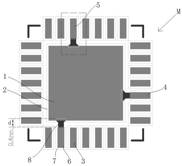
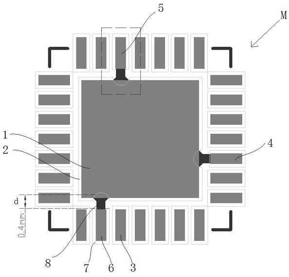
[0037] The QFN chip PCB package method of the present invention and a PCB plate designed according to this method are provided with a pad for welding QFN chips, the pad including an intermediate pad and a plurality of leads in the intermediate pad. Foot pad. The present invention can thoroughly solve the problem of welding when the pin of the chip is connected to the PCB intermediate pad, but also guarantees that the performance of the chip itself is unaffected, thereby improving the reliability of the product and reducing market adverseity.
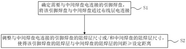
[0038] The QFN chip PCB package method of this embodiment includes the following steps, see figure 1 Indicated.
[0039] Step S1: Determine the pin pad that is electrically connected to the intermediate pad, electrically co...
PUM
 Abstract
Description
Claims
Application Information