PCB packaging structure based on light-weight miniature smt components

A technology of packaging structure and components, which is applied in the direction of printed circuits connected with non-printed electrical components, electrical connection printed components, printed circuit components, etc., which can solve the problems of electromagnetic radiation, short circuit with tin, poor welding, etc. problems, achieve the effect of reducing the risk of tin connection, preventing electromagnetic interference, and reducing production costs

Active Publication Date: 2017-02-22
深圳市磊科实业有限公司
View PDF7 Cites 0 Cited by
  • Summary
  • Abstract
  • Description
  • Claims
  • Application Information

AI Technical Summary

Problems solved by technology

[0007] The purpose of the present invention is to provide a PCB packaging structure based on light-weight miniature SMT components, which mainly solves the problems of soldering short circuit, poor welding and easy generation of electromagnetic waves in the PCB packaging of existing light-weight miniature SMT components during the pad layout process. radiation source problem

Method used


Image

  • PCB packaging structure based on light-weight miniature smt components
  • PCB packaging structure based on light-weight miniature smt components
  • PCB packaging structure based on light-weight miniature smt components

Examples


Embodiment

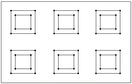
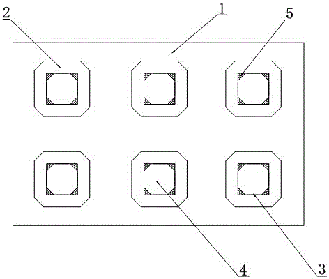
[0026] like figure 2 As shown, the present invention is mainly aimed at the PCB packaging of 0201, 0402, 0603, 0805, 1206, 1210 types of light-weight miniature SMT components, which include PCB substrate 1, SMT solder mask window 2 and SMT pad 4 . There are at least two windows in the SMT solder resist layer, which are straightened and evenly distributed on the PCB substrate 1 , and each window 2 in the SMT solder resist layer is provided with a square pad window 3 . The SMT pad 4 is arranged in the square pad opening 3, and the SMT pad 4 is a symmetrical octagonal structure formed by end-to-end connection of four equal long sides 41 and four equal hypotenuses 42, wherein the SMT pad The four long sides of 4 correspond to the four sides of the square pad opening 3 one by one, and the angle between the hypotenuse of the SMT pad and the long side is greater than 90°. The shape and arrangement of the outer edge of the window 2 in the SMT solder resist layer are the same as tho...


PUM


Abstract

The invention discloses a PCB packaging structure based on a light-quality SMT component. The PCB packaging structure comprises a PCB substrate, at least two SMT solder mask layer windows which are straightened to be uniformly distributed on the PCB substrate and are provided with square pad windows, and an SMT pad which is arranged in the square pad window. The SMT pad is of a symmetrical octagon structure formed by connecting four equal long edges with four equal inclined edges in an end-to-end manner. The four long edges of the SMT pad are closely attached to the four edges of the square pad windows in one-to-one correspondence, the four inclined edges of the SMT pad are in one-to-one-correspondence with the four corners of the square pad window, the included angles between the inclined edges of the SMT pad and the long edges of the SMT pad are greater than 90 degrees, and the outer edges of the SMT solder mask layer windows have the same shape and arrangement modes as the SMT pad. The advantages are as follows: the structural design is reasonable, an electromagnetic radiation source can be effectively prevented from generating, and the problems of tin connection short circuits and insufficient welding or false welding are well solved.

Description

technical field [0001] The invention relates to a PCB packaging structure, in particular to a PCB packaging structure based on light-weight miniature SMT components. Background technique [0002] At present, for the PCB packaging structure of light-weight micro-miniature SMT components (such as 0201, 0402, 0603, 0805, 1206, 1210), there are the following defects in the pad layout process: [0003] (1) The window of the SMT solder mask layer and the SMT pad are usually of a regular quadrilateral or rectangular design, the SMT pad is set in the square pad window, and the four sides of the SMT pad are close to the four sides corresponding to the square pad window , In this way, the copper foil of the PCB board itself will cause electromagnetic radiation sources in the copper-clad area due to the existence of sharp or isolated areas of ≤90° (such as figure 1 Indicated by the black dot in), and then electromagnetic interference (EMI) occurs. [0004] (2) Due to the volume and a...

Claims


Application Information

Patent Timeline
Patent Type & Authority Patents(China)
IPC IPC(8): H05K1/11H05K1/18
Inventor 朱福林
Owner 深圳市磊科实业有限公司
Why Eureka
Try Eureka