Trench gate igbt device with high short-circuit resistance and preparation method thereof

A technology of trench gate and manufacturing method, applied in the field of microelectronics, can solve the problems of reducing the short-circuit resistance of the device, increasing the IGBT current, affecting the normal application of the device, etc., and achieving the effect of improving the short-circuit resistance, reducing the saturation current and having a compact structure

Active Publication Date: 2020-03-17
GLOBAL ENERGY INTERCONNECTION RES INST CO LTD +3
View PDF7 Cites 0 Cited by
  • Summary
  • Abstract
  • Description
  • Claims
  • Application Information

AI Technical Summary

Problems solved by technology

[0003] But the trench gate IGBT also has its disadvantages: a wider conductive channel will increase the current when the IGBT is short-circuited and reduce the short-circuit resistance of the device
At present, the main methods to increase the short-circuit resistance of trench-gate IGBTs are: increasing the trench spacing, reducing the channel density, and reducing the saturation current, but this is accompanied by weakening of the withstand voltage capability; using a dummy trench structure, the usual method is to make the dummy region The gate of the gate is disconnected from the real trench gate, connected to the emitter or floating, these methods will always involve changes in the parasitic capacitance of the device, which will lead to various oscillations during the switching process, and then affect the device's performance. normal application

Method used


Image

  • Trench gate igbt device with high short-circuit resistance and preparation method thereof
  • Trench gate igbt device with high short-circuit resistance and preparation method thereof
  • Trench gate igbt device with high short-circuit resistance and preparation method thereof

Examples


Embodiment Construction

[0038] The present invention will be further described below in conjunction with specific drawings and embodiments.

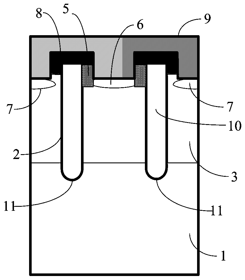
[0039] Such as figure 1 and Figure 10Shown: In order to reduce the channel density of the trench gate IGBT, reduce the saturation current, and effectively improve the short-circuit resistance capability of the trench gate IGBT without affecting the withstand voltage and parasitic capacitance of the IGBT device, the N-type IGBT device is used as the For example, the present invention includes a semiconductor base and a cell region located in the central region of the semiconductor substrate, and the semiconductor substrate includes an N-type base region 1 and a P-type base region 3 directly above the N-type base region 1;

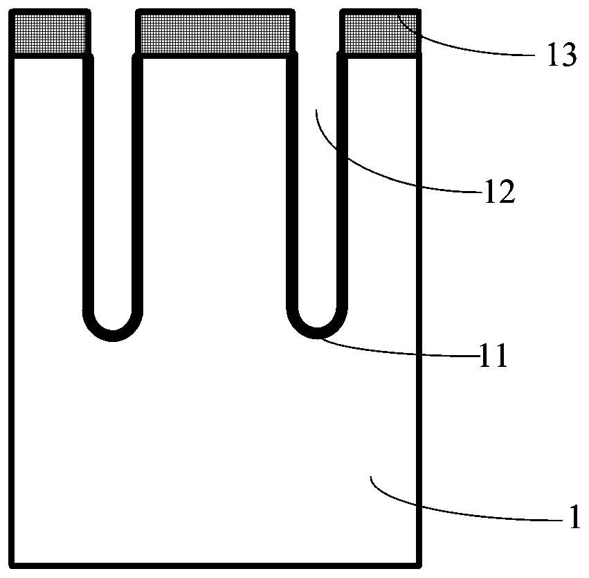
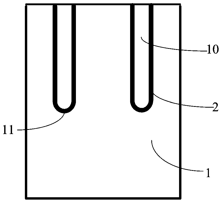
[0040] The cells in the cell area include two adjacent cell grooves 11, the cell grooves 11 are located in the P-type base region 3, and the depth of the cell grooves 11 extends into the N below the P-type base region 3. In the base region...


PUM

PropertyMeasurementUnit
depthaaaaaaaaaa
widthaaaaaaaaaa
depthaaaaaaaaaa

Abstract

The invention relates to a trench gate IGBT device with high anti-short circuit capability and a preparation method thereof. A cell in a cell region comprises two adjacent cell trenches. A first bodyregion of a second conductivity type is arranged above adjacent outer side walls of two adjacent cell trenches. The first body region of the second conductivity type contacts the side wall of the corresponding cell trench. A first conductivity type source region is arranged above the outer side walls, which are spaced apart from each other, of two adjacent cell trenches. The first conductivity type source region contacts the side wall of the corresponding cell trench. When the first body region of the second conductivity type is manufactured, a lithography plate injected into the first conductivity type source region is simply adjusted. Without affecting the withstand voltage and the parasitic capacitance of the IGBT device, the channel density of the trench gate IGBT is reduced. Saturation current is reduced. The short circuit resistance of the trench gate IGBT device is effectively improved. The trench gate IGBT device has the advantages of compact structure and being safe and reliable, and is compatible with the existing technology.

Description

technical field [0001] The invention relates to a trench gate IGBT device and a preparation method thereof, in particular to a trench gate IGBT device with high short-circuit resistance and a preparation method thereof, belonging to the technical field of microelectronics. Background technique [0002] The planar gate IGBT has a JFET structure and the weak conductance modulation effect of the emitter region. For the planar gate IGBT, the carrier concentration gradually decreases from the collector to the emitter. The design goal of the new generation of IGBT is to maintain a uniform distribution of carrier concentration, preferably gradually increased, which can further reduce the on-state loss without affecting the tail current and turn-off loss, which leads to the emergence of trench gate structure . Compared with the planar gate IGBT, the conductive channel of the vertical structure of the trench gate IGBT is more conducive to the design of compact cells, that is, more I...

Claims


Application Information

Patent Timeline
Patent Type & Authority Patents(China)
IPC IPC(8): H01L29/739H01L21/331H01L29/10
Inventor 金锐杨晓鸾许生根姜梅董少华崔磊
Owner GLOBAL ENERGY INTERCONNECTION RES INST CO LTD
Why Eureka
Try Eureka