An AMOLED pixel drive circuit and a driving method thereof

A pixel driving circuit and potential technology, applied in instruments, static indicators, etc., can solve the problems of a large number of scanning control signals, a low pixel effective light-emitting area, and a complex timing controller, so as to increase the effective light-emitting area and improve the display. effect, current stabilization effect

Active Publication Date: 2018-02-02
SHENZHEN CHINA STAR OPTOELECTRONICS SEMICON DISPLAY TECH CO LTD
View PDF5 Cites 4 Cited by
  • Summary
  • Abstract
  • Description
  • Claims
  • Application Information

AI Technical Summary

Problems solved by technology

[0005] like figure 1 As shown, an AMOLED pixel driving circuit with a 7T2C structure includes 7 thin film transistors and 2 capacitors, which are respectively: a first thin film transistor T10, a second thin film transistor T20, a third thin film transistor T30, a fourth thin film transistor T40, The fifth thin film transistor T50, the sixth thin film transistor T60, the seventh thin film transistor T70, the first capacitor C10, and the second capacitor C20, the pixel drive circuit needs to be controlled by four scan control signals, which are the first scan control signal S10, The second scan control signal S20, the third scan control signal S30, and the fourth scan control signal S40; the working timing diagram of the circuit is as follows figure 2 As shown, the working process of the circuit includes: a first stage 10, a second stage 20, and a third stage 30, wherein in the second stage 20, the second scanning control signal S20 first provides a high potential and then provides a low potential, and this When the second scanning control signal S20 provides a low potential, due to the effect of the first capacitor C1, the potential at the connection point between the first capacitor C1 and the second capacitor C2 will be unstable, and the pixel driving circuit needs 7 One thin film transistor and two capacitors, the structure is complex, the effective light-emitting area of ​​the pixel is low, and the number of scanning control signals is large, which makes the timing controller more complicated

Method used


Image

  • An AMOLED pixel drive circuit and a driving method thereof
  • An AMOLED pixel drive circuit and a driving method thereof
  • An AMOLED pixel drive circuit and a driving method thereof

Examples


Embodiment Construction

[0048] In order to further illustrate the technical means adopted by the present invention and its effects, the following describes in detail in conjunction with preferred embodiments of the present invention and accompanying drawings.

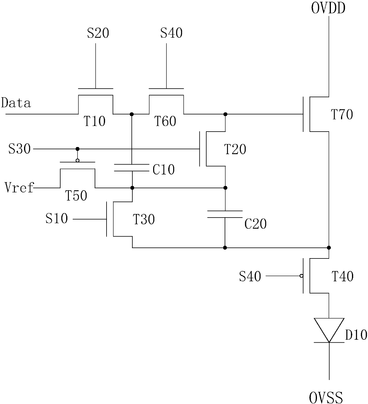
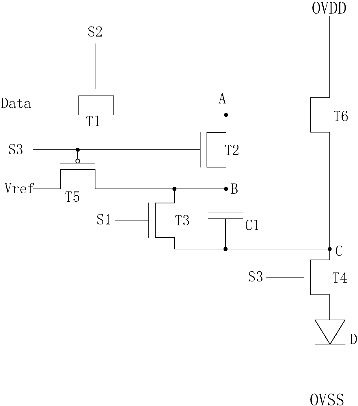
[0049] see image 3 , the present invention provides an AMOLED pixel drive circuit, comprising: a first thin film transistor T1, a second thin film transistor T2, a third thin film transistor T3, a fourth thin film transistor T4, a fifth thin film transistor T5, a sixth thin film transistor T6, a capacitor C1, and organic light emitting diode D;

[0050] The gate of the first thin film transistor T1 is connected to the second scanning control signal S2, the source is electrically connected to the data signal Data, and the drain is electrically connected to the first node A;

[0051] The gate of the second thin film transistor T2 is connected to the third scanning control signal S3, the source is electrically connected to the first node A, and...


PUM


Abstract

The invention provides an AMOLED pixel drive circuit and a driving method thereof. The pixel drive circuit with a 6T1C structure is employed with a specific drive time sequence, so that threshold voltages for driving thin film transistors can be effectively compensated for and currents flowing through organic light emitting diodes are stable, the light emitting brightness of the organic light emitting diodes is uniform and an image display effect is improved; through the cooperation of N-type thin film transistors and P-type thin film transistors, the numbers of thin film transistors and scanning control signals are reduced, the structure of the pixel drive circuit is simplified and an effective light emitting area is increased.

Description

technical field [0001] The invention relates to the field of display technology, in particular to an AMOLED pixel driving circuit and a driving method thereof. Background technique [0002] Organic light emitting diode (Organic Light Emitting Display, OLED) display device has self-illumination, low driving voltage, high luminous efficiency, short response time, high definition and contrast, nearly 180° viewing angle, wide operating temperature range, and can realize flexible display and With many advantages such as large-area full-color display, it is recognized by the industry as a display device with the most potential for development. [0003] OLED display devices can be divided into passive matrix OLED (Passive Matrix OLED, PMOLED) and active matrix OLED (Active Matrix OLED, AMOLED) two categories according to the driving method, namely direct addressing and thin film transistor (Thin Film Transistor, TFT) matrix addressing two types. Among them, AMOLED has pixels arra...

Claims


Application Information

Patent Timeline
Patent Type & Authority Applications(China)
IPC IPC(8): G09G3/3233G09G3/3266
CPCG09G3/3233G09G3/3266G09G2320/0233G09G2300/0819G09G2300/0852G09G2300/0861G09G2310/0251G09G2310/0262G09G2310/08G09G2320/043G09G2320/045
Inventor 王珊温亦谦
Owner SHENZHEN CHINA STAR OPTOELECTRONICS SEMICON DISPLAY TECH CO LTD
Why Eureka
Try Eureka