Semiconductor laser module and packaging method thereof

A packaging method and laser technology, applied in the direction of semiconductor lasers, lasers, laser components, etc., can solve the problems of high power of laser chips, affecting device reliability, high current density, etc., and achieve large contact area, improve reliability, and heat dissipation fast effect

Inactive Publication Date: 2018-02-02
SUZHOU EVERBRIGHT PHOTONICS CO LTD
View PDF3 Cites 0 Cited by
  • Summary
  • Abstract
  • Description
  • Claims
  • Application Information

AI Technical Summary

Problems solved by technology

However, due to the high power of the laser chip and the high current density passing through it, the lead wires of the traditional microchannel water-cooled semiconductor laser module often break during use, which causes the device to burn out and seriously affects the reliability of the device.

Method used


Image

  • Semiconductor laser module and packaging method thereof
  • Semiconductor laser module and packaging method thereof
  • Semiconductor laser module and packaging method thereof

Examples


Embodiment Construction

[0025] The implementation of the present invention will be described in detail below in conjunction with the accompanying drawings and examples, so as to fully understand and implement the process of how to apply technical means to solve technical problems and achieve technical effects in the present invention. It should be noted that, as long as there is no conflict, each embodiment and each feature in each embodiment of the present invention can be combined with each other, and the formed technical solutions are all within the protection scope of the present invention.

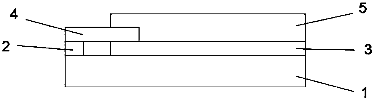
[0026] Such as Figure 1-4 As shown, the embodiment of the present application provides a semiconductor laser module, which includes: a microchannel heat sink 1 , a laser chip 2 , an insulating adhesive film 3 , a first cathode sheet 4 and a second cathode sheet 5 .

[0027] In the embodiment of the present application, the positive electrode of the laser chip 2 is connected to the negative electrode of the ...


PUM


Abstract

The invention discloses a semiconductor laser module and a packaging method thereof. The module comprises a microchannel heat sink (1), a laser chip (2), an insulating adhesive film (3), a first cathode sheet (4) and a second cathode sheet (5). The positive electrode of the laser chip (2) is connected with the microchannel heat sink (1) in a soldering way through a first solder. The negative electrode of the laser chip (2) is connected with the first cathode sheet (4) in a soldering way through a second solder. The first cathode sheet (4) is connected with the second cathode sheet (5). The insulating adhesive film (3) is arranged between the second cathode sheet and the microchannel heat sink. Compared with the conventional lead bonding mode, the packaging method is simple in technology, the contact area of the connection mode of the negative electrode of the laser chip and the first cathode sheet through the solder is large and heat radiation is fast without the situation of device burnout caused by disconnection so that the stability and the reliability of the device can be enhanced.

Description

technical field [0001] The invention belongs to the field of laser testing, and belongs to a semiconductor laser module and a packaging method thereof. Background technique [0002] At present, semiconductor laser modules can be divided into micro-channel water cooling, macro-channel water cooling and conduction cooling according to cooling methods. The microchannel water-cooled semiconductor laser module includes a microchannel heat sink, a laser chip, an insulating adhesive film, and a cathode sheet. Between the cathode sheet and the microchannel heat sink, it plays an insulating role. However, due to the high power of the laser chip and the high current density passing through it, the lead wires of the traditional microchannel water-cooled semiconductor laser module often break during use, which causes the device to burn out and seriously affects the reliability of the device. Contents of the invention [0003] The technical problem to be solved by the present inventi...

Claims


Application Information

Patent Timeline
Patent Type & Authority Applications(China)
IPC IPC(8): H01S5/024H01S5/042H01S5/022
CPCH01S5/02423H01S5/0425H01S5/0237
Inventor 朱滨
Owner SUZHOU EVERBRIGHT PHOTONICS CO LTD
Why Eureka
Try Eureka