Semiconductor device
A technology for semiconductors and thick-walled parts, which is used in semiconductor devices, semiconductor/solid-state device components, and electric solid-state devices. Increase in size, reducing the effect of thermal interference
- Summary
- Abstract
- Description
- Claims
- Application Information
AI Technical Summary
Problems solved by technology
Method used
Image

Examples
Embodiment approach 1
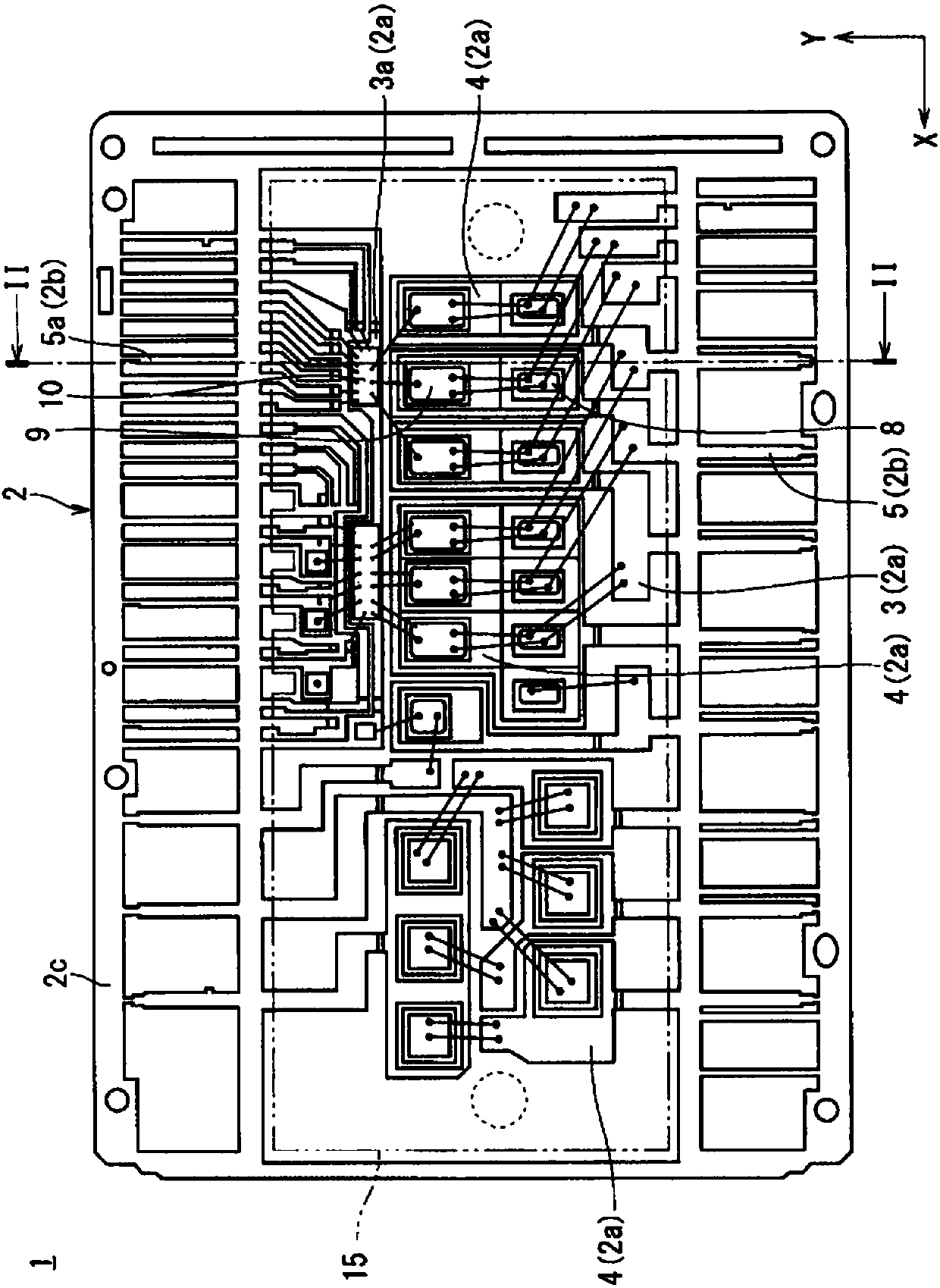
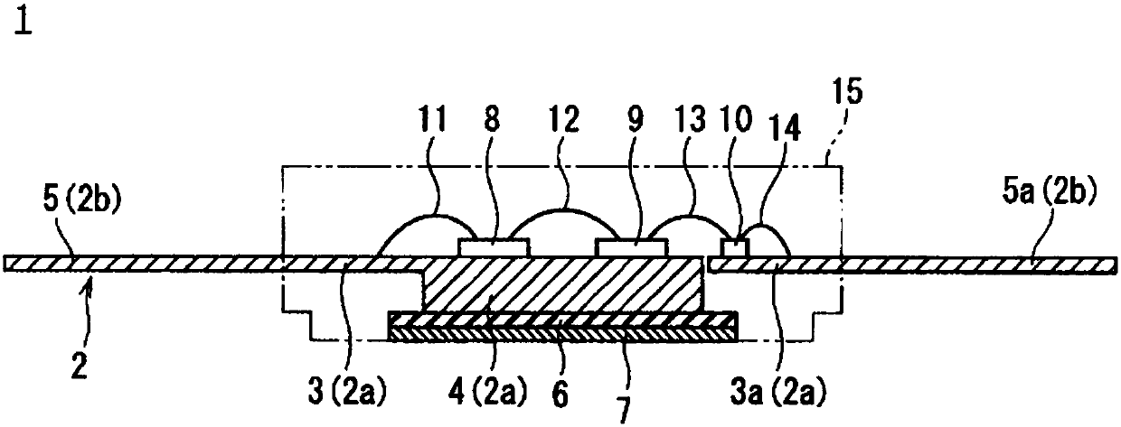
[0025] Next, Embodiment 1 of the present invention will be described using the drawings. figure 1 It is a plan view of the semiconductor device 1 according to the first embodiment. figure 2 is a cross-sectional view of the semiconductor device 1, more specifically, is figure 1 The II-II line sectional view. it's here, figure 1 It is a drawing showing before the connecting rod cutting process. In addition, toward figure 1 , the left-right direction will be described as the X-axis direction, and the up-down direction will be described as the Y-axis direction.
[0026] Such as figure 1 and figure 2 As shown, the semiconductor device 1 is, for example, a power module, and includes power chips 8 and 9 , an IC chip 10 , a lead frame 2 , a molding resin 15 , an insulating layer 6 , and a heat sink 7 . The lead frame 2 includes: an inner lead 2a encapsulated by a molding resin 15; an outer lead 2b connected to the inner lead 2a; and an outer frame portion 2c connected to the ...
Embodiment approach 2
[0045] Next, a semiconductor device 1A according to Embodiment 2 will be described. Figure 5 It is a cross-sectional view of the semiconductor device 1A according to the second embodiment. In addition, in Embodiment 2, the same constituent elements as those already described in Embodiment 1 are given the same reference numerals, and description thereof will be omitted. In addition, in Figure 5 The illustration of the molding resin 15 is omitted hereafter.
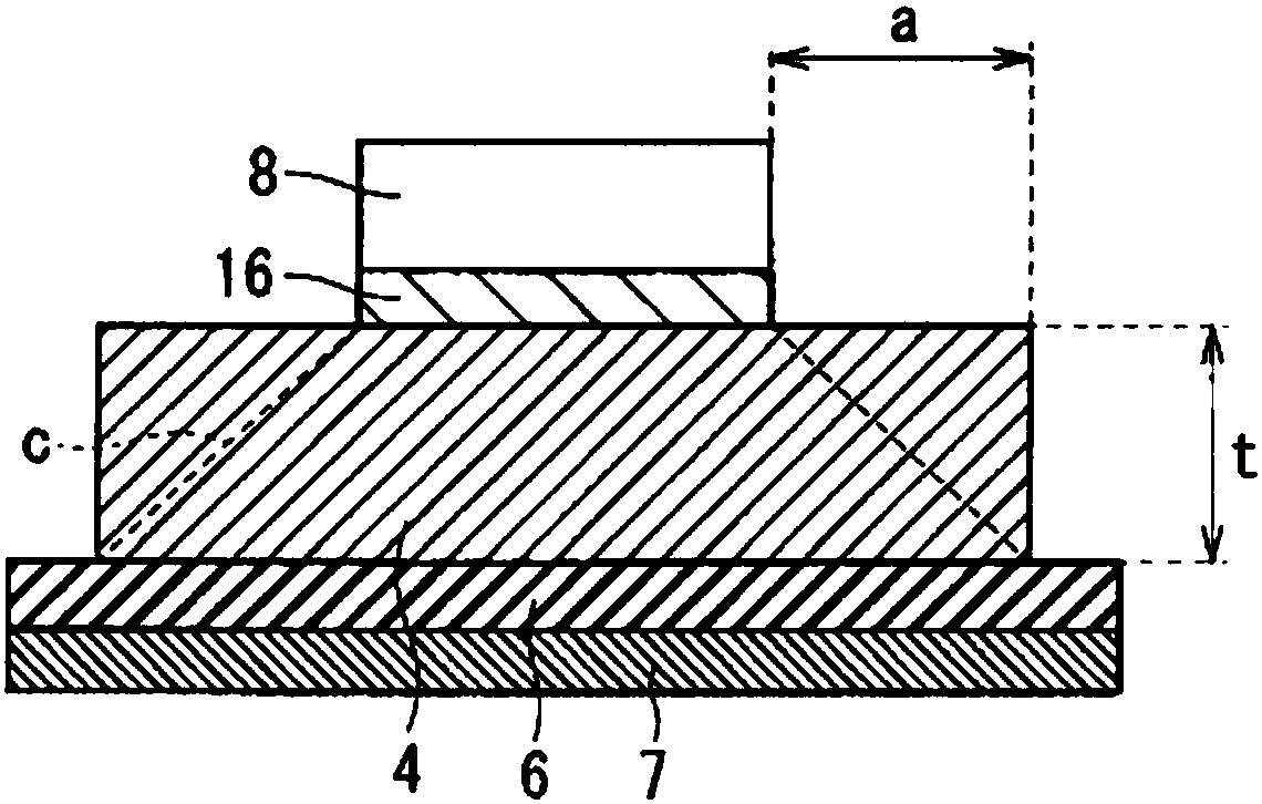
[0046] Such as Figure 5 As shown, in the second embodiment, the structure in which the thick portion 4 is sunk downward is employed. More specifically, by fixing the connection portion of the thin portion 3 with the thick portion 4 in a state of being bent downward, the upper surface of the thick portion 4 is placed on the upper surface of the thinner portions 3, 3a. The height position of the surface is low.
[0047] And, if the sum of the sinking dimension of the thick-walled portion 4 and the thickness of the thi...
Embodiment approach 3
[0051] Next, a semiconductor device 1B according to Embodiment 3 will be described. Figure 6 It is a cross-sectional view of the semiconductor device 1B according to the third embodiment. In addition, in Embodiment 3, the same components as those already described in Embodiments 1 and 2 are assigned the same reference numerals and description thereof will be omitted.
[0052] Such as Figure 6 As shown, in Embodiment 3, the thick portion 4 and the thin portions 3, 3a are formed of different members, and the thick portion 4 is formed of a member having higher thermal conductivity than the thin portions 3, 3a. More specifically, the thick portion 4 includes: a first member 4a arranged on the lower surface of the thin portion 3; and a second member 4b arranged on the lower surface of the first member 4a. Here, the first member 4a is formed of, for example, silver, and the second member 4b is formed of, for example, pure copper. Alternatively, the first member 4a may be formed...
PUM
 Abstract
Description
Claims
Application Information
 - R&D
- Intellectual Property
- Life Sciences
- Materials
- Tech Scout
- Unparalleled Data Quality
- Higher Quality Content
- 60% Fewer Hallucinations
Browse by: Latest US Patents, China's latest patents, Technical Efficacy Thesaurus, Application Domain, Technology Topic, Popular Technical Reports.
© 2025 PatSnap. All rights reserved.Legal|Privacy policy|Modern Slavery Act Transparency Statement|Sitemap|About US| Contact US: help@patsnap.com