Light-emitting diode and manufacturing method thereof

A technology for light-emitting diodes and a manufacturing method, which can be applied to semiconductor devices, electrical components, circuits, etc., and can solve problems such as low carrier mobility and current congestion.

Pending Publication Date: 2018-02-09
XIAMEN SANAN OPTOELECTRONICS TECH CO LTD
View PDF1 Cites 26 Cited by
  • Summary
  • Abstract
  • Description
  • Claims
  • Application Information

AI Technical Summary

Problems solved by technology

In GaN LEDs, p-GaN usually causes some current congestion at the bottom of the pad due to its low carrier mobility

Method used


Image

  • Light-emitting diode and manufacturing method thereof
  • Light-emitting diode and manufacturing method thereof
  • Light-emitting diode and manufacturing method thereof

Examples


Embodiment 1

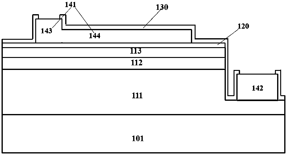
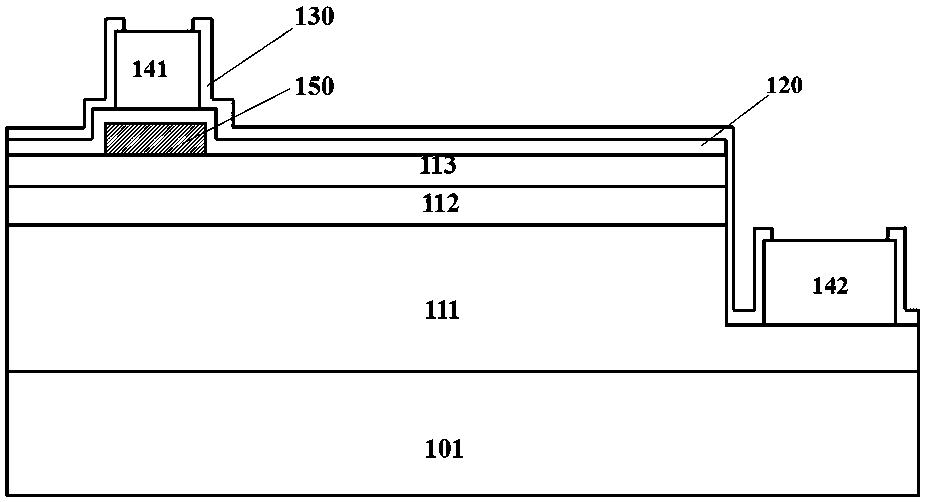
[0130] Such as image 3 As shown, a light-emitting diode includes: a substrate 201 , an N-type layer 211 , a light-emitting layer 212 , a P-type layer 213 , a transparent conductive layer 220 , a semiconductor protection layer 230 , a first electrode 241 , and a second electrode 242 .

[0131] Specifically, the substrate 201 includes but is not limited to sapphire, aluminum nitride, gallium nitride, silicon, and silicon carbide, and its surface structure can be a planar structure or a patterned pattern structure; the N-type layer 211 is formed on the sapphire substrate 201 on; the light-emitting layer 212 is formed on the N-type layer 211; the P-type layer 213 is formed on the light-emitting layer 212; the transparent conductive layer 220 is formed on the P-type layer 213; the semiconductor protection layer 230 is formed on the transparent conductive layer 220; the first The electrode 241 and the second electrode 242 are formed on the semiconductor protection layer 230 . Fig...

Embodiment 2

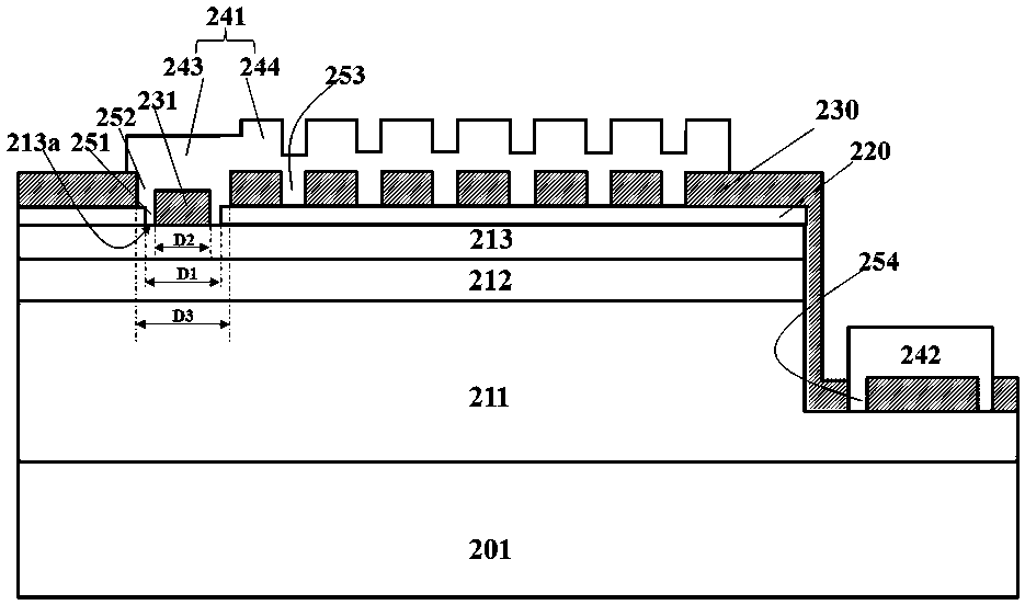
[0138] This embodiment discloses a method for manufacturing a light-emitting diode, which mainly includes four processes of mesa etching (MESA), making a transparent conductive layer, making a semiconductor protective layer, and making an electrode. Figure 5 It is shown that the four processes involve respective corresponding mask patterns. Combine below Figure 5-8 Give a brief explanation.

[0139] First, a light-emitting epitaxial layer structure is provided, which generally includes a substrate 201 , an N-type layer 211 , a light-emitting layer 212 , and a P-type layer 213 .

[0140] Next, refer to Figure 5The pattern shown in (a) defines the first electrode region and the second electrode region on the surface of the light-emitting epitaxial layer, removes the hole region, forms the mesa 210 of the second electrode and a series of through holes 256, as Figure 6 shown;

[0141] Next, refer to Figure 5 In the pattern shown in (b), a transparent conductive layer 220...

Embodiment 3

[0146] Figure 9 A schematic diagram showing the structure of another light-emitting diode. The difference from Embodiment 1 is that in the light-emitting diode structure described in this embodiment, the diameter D1 of the second opening 252 is greater than or equal to the diameter D1 of the first opening. At this time, there is no The semiconductor protection layer is in direct contact with the P-type layer 213. At this time, the pad part of the first electrode is in direct contact with the semiconductor, and the adhesion between the electrode and the GaN interface is good, which can reduce the risk of detachment between the first electrode and the adhesion interface of the wire bonding .


PUM


Abstract

The invention discloses a light-emitting diode and a manufacturing method thereof. The light-emitting diode comprises a light-emitting epitaxial layer, a transparent conductive layer, a protection layer and a first electrode, wherein the light-emitting epitaxial layer sequentially comprises a first semiconductor layer, a light-emitting layer and a second semiconductor layer from top to bottom; a first electrode area is arranged on the upper surface of the light-emitting epitaxial layer; the first electrode area comprises a bonding pad area and an expansion area; the transparent conductive layer is formed on the surface of the first semiconductor layer of the light-emitting epitaxial layer, a first opening is formed in the bonding pad area, and the surface, in the bonding pad area, of the first semiconductor layer is exposed; the protection layer is formed on the surface of the transparent conductive layer, a second opening and a third opening are formed in the bonding pad area and theexpansion area of the first electrode area separately, and the surface, in the bonding pad area, of the first semiconductor layer and the surface, in the expansion area, of the transparent conductivelayer are exposed; and the first electrode is formed on the protection layer, and is in direct contact with the first semiconductor layer of the bonding pad area through the first opening and the second opening.

Description

technical field [0001] The invention relates to a semiconductor element, in particular to a light emitting diode and a manufacturing method thereof. Background technique [0002] Due to the advantages of long life, small size, high shock resistance, low heat generation and low power consumption, light-emitting diodes have been widely used in home appliances and indicators or light sources of various instruments. [0003] The early gallium nitride LED chip manufacturing process usually consists of four processes: mesa etching (MESA), making a transparent conductive layer (such as ITO), making electrodes and making a protective layer. The light-emitting diode chips formed by it are as follows: figure 1 As shown, it generally includes a substrate 101, an N-type layer 111, a light emitting layer 112, a P-type layer 113, a transparent conductive layer 120, a P electrode 141 (pad 143 and an extension bar 144), an N electrode 142 and a protective layer 130. In GaN LEDs, p-GaN typi...

Claims


Application Information

Patent Timeline
Patent Type & Authority Applications(China)
IPC IPC(8): H01L33/14H01L33/38H01L33/46H01L33/00
CPCH01L33/0075H01L33/145H01L33/38H01L33/46H01L2933/0016H01L2933/0025H01L33/42H01L33/14H01L33/62H01L27/153H01L33/10
Inventor 林素慧洪灵愿许圣贤陈思河陈大钟陈功张家宏彭康伟
Owner XIAMEN SANAN OPTOELECTRONICS TECH CO LTD
Why Eureka
Try Eureka