A luminescent part for laser GaN base peeling based on compound separation method and its making method

A light-emitting device, laser lift-off technology, applied in the direction of semiconductor devices, electrical components, circuits, etc., can solve the problems of high production rate, prone to cracks, damage to light-emitting devices, etc., to reduce the production rate of cracks, avoid crack extension, improve The effect of yield

Active Publication Date: 2008-08-13
XIAMEN SANAN OPTOELECTRONICS TECH CO LTD
View PDF0 Cites 20 Cited by
  • Summary
  • Abstract
  • Description
  • Claims
  • Application Information

AI Technical Summary

Problems solved by technology

However, this method has the following problems: First, the total thickness of the GaN-based epitaxial layer is generally between 4-10 μm. If the entire GaN-based epitaxial layer is simply removed by dry etching, there are disadvantages such as difficulty in implementing the etching process and poor repeatability. , and it is difficult to judge whether the GaN-based epitaxial layer is completely removed, so it is difficult to achieve absolute separation of GaN-based light-emitting devices in each unit, resulting in a high rate of cracks in the laser lift-off process; The epitaxial layer forms a plurality of separated GaN-based light-emitting devices. Although it is easy to achieve absolute isolation, it will introduce the degradation of the electrical and optical properties of GaN-based light-emitting devices caused by laser; Taking the scanning irradiation method, the overlapped irradiation area of ​​the laser beam is prone to cracks, and the cracks and damage here may extend and destroy its light-emitting devices

Method used


Image

  • A luminescent part for laser GaN base peeling based on compound separation method and its making method
  • A luminescent part for laser GaN base peeling based on compound separation method and its making method
  • A luminescent part for laser GaN base peeling based on compound separation method and its making method

Examples


Embodiment Construction

[0036] The present invention will be further described below in conjunction with the accompanying drawings and embodiments.

[0037] A method for manufacturing laser lift-off GaN-based light-emitting devices using a synthetic separation method, the steps of which are as follows:

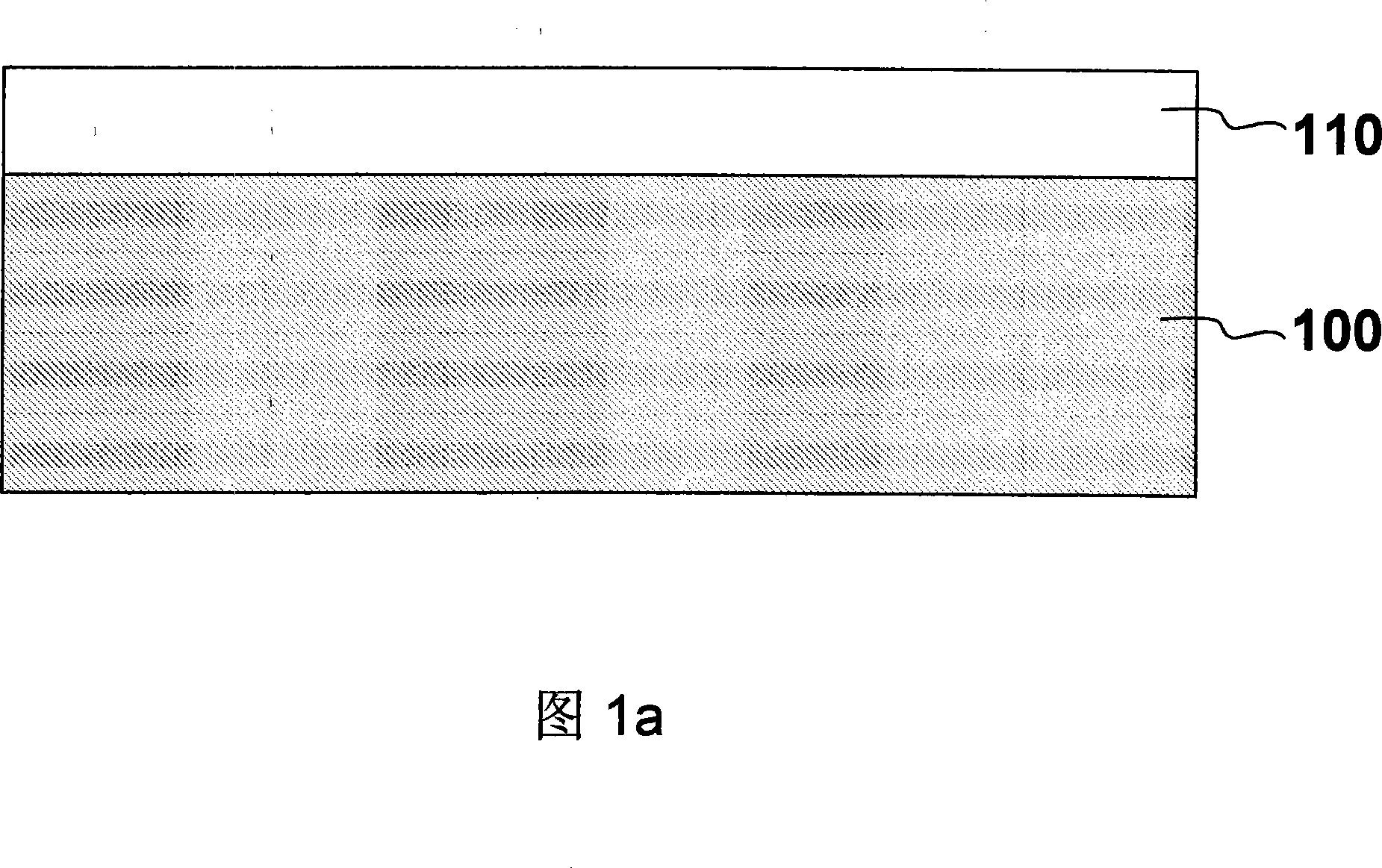
[0038] Step 1: First, as shown in FIG. 1a, a nitride semiconductor epitaxial film 110 is heteroepitaxially grown on a sapphire substrate 100, and the epitaxial film 110 has an N-GaN layer, an active layer and a P-GaN layer.

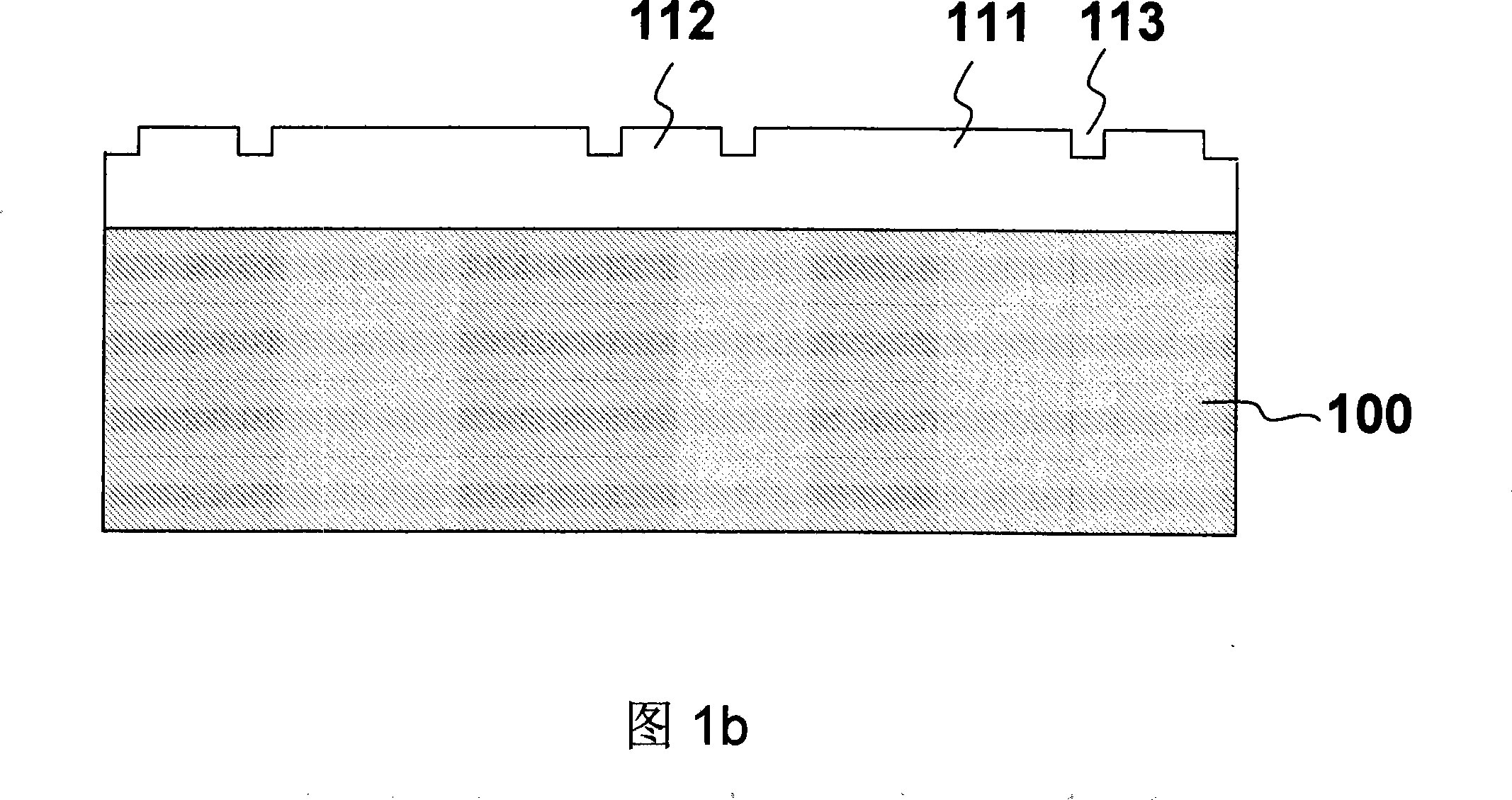
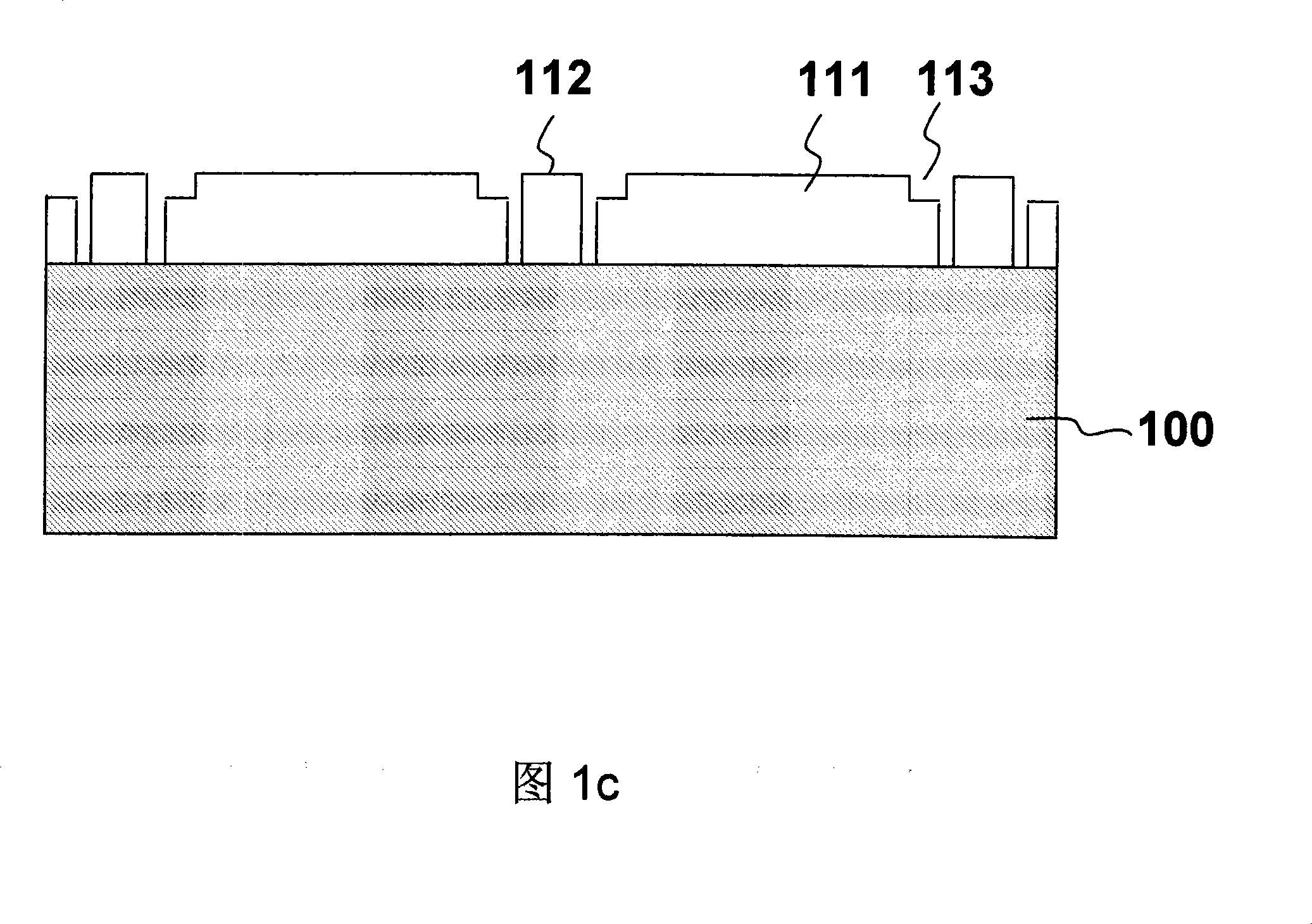
[0039] Step 2: firstly use dry etching to remove part of the GaN-based epitaxial layer at predetermined intervals, and form a plurality of GaN-based light emitting regions 111 and 112 of two different sizes on the epitaxial film 110 of the sapphire substrate 100, as shown in the figure As shown in 1b, the unit GaN-based light-emitting region 111 has a width of more than 300 μm, the unit GaN-based light-emitting region 112 has a width of 40-200 μm, the depth of the groove 113 for...


PUM

PropertyMeasurementUnit
thicknessaaaaaaaaaa
thicknessaaaaaaaaaa
thicknessaaaaaaaaaa

Abstract

A laser stripping GaN base illuminating device which is disclosed in the invention and is applied with a synthesizing separating method and the manufacturing method adopt the synthesizing separating method for separating each unit GaN base illuminating device, combining the method for eliminating partial GaN base epitaxial layer and laser-gashing the GaN base epitaxial layer with the dry method, the absolute separating between each unit GaN base illuminating devices can be guaranteed, the creation rate of the slit in the laser stripping process is reduced, and the capability of the device can be protected from being damaged in the laser insulating process; an area is preserved between each of unit GaN base illuminating devices as a laser stripping sacrificial area and is insulated from the unit illuminating device to avoid the extending of the fracture and the illuminating device damage generated by the overlapping irradiation of the laser beam in the laser stripping process and increase the finished product rate of the illuminating device after laser stripping; the laser stripping sacrificial area is surrounded by a metal ring and after laser stripping the residue of epitaxial layer in the sacrificial area can be easily removed along with the etching of the metal ring.

Description

technical field [0001] The invention relates to a GaN-based semiconductor light-emitting device and a manufacturing method thereof, in particular to a GaN-based light-emitting device and a manufacturing method thereof which are laser-stripped by a composite separation method. Background technique [0002] At present, most GaN-based epitaxy is mainly grown on sapphire substrates. Due to the poor conductivity of sapphire, ordinary GaN-based light-emitting devices adopt a lateral structure, that is, the two electrodes are on the same side of the device, and the current flows laterally in the N-GaN layer. Flowing at unequal distances, there is current blockage and heat generation; in addition, the thermal conductivity of the sapphire substrate is low, thus limiting the luminous power and efficiency of GaN-based devices. [0003] Removing the sapphire and making the light-emitting device into a vertical structure can effectively solve the problems of heat dissipation, light outpu...

Claims


Application Information

Patent Timeline
Patent Type & Authority Applications(China)
IPC IPC(8): H01L33/00
Inventor 吴志强林雪娇潘群峰洪灵愿陈文欣
Owner XIAMEN SANAN OPTOELECTRONICS TECH CO LTD
Why Eureka
Try Eureka