A semiconductor chip self-alignment pendulum

A self-aligned, semiconductor technology, applied in the field of optoelectronics, can solve the problems of laser qualification rate and yield, heat sink and shell sintering cavity, complex structure of sintering fixture, etc. Low cost and simple structure

Active Publication Date: 2019-10-08
BEIJING UNIV OF TECH
View PDF18 Cites 0 Cited by
  • Summary
  • Abstract
  • Description
  • Claims
  • Application Information

AI Technical Summary

Problems solved by technology

Commonly used sintering equipment with manual swing and suction nozzle pressurization is single-point pressurization, the pressure is uneven, and the solder will have a certain fluidity when melting, which will cause sintering voids between the heat sink and the shell.
[0003] The structure of the conventional sintering fixture is as complicated as the patent 201520453486.4
The fixture with a relatively simple structure can only place one die at a time, which is inefficient, such as patent 201610285100.2
At the same time, the above equipment is not suitable for operation in a nitrogen hood, and it is prone to the problem of cavity surface oxidation, which will affect the pass rate and yield of the laser.
Moreover, the general swing device needs to turn the die with the P side down, and these operations will cause mechanical damage

Method used


Image

  • A semiconductor chip self-alignment pendulum
  • A semiconductor chip self-alignment pendulum
  • A semiconductor chip self-alignment pendulum

Examples


Embodiment Construction

[0024] In order to make the object, technical solution and advantages of the present invention clearer, the present invention will be further described in detail below in conjunction with a simple etching structure as a specific embodiment and with reference to the accompanying drawings.

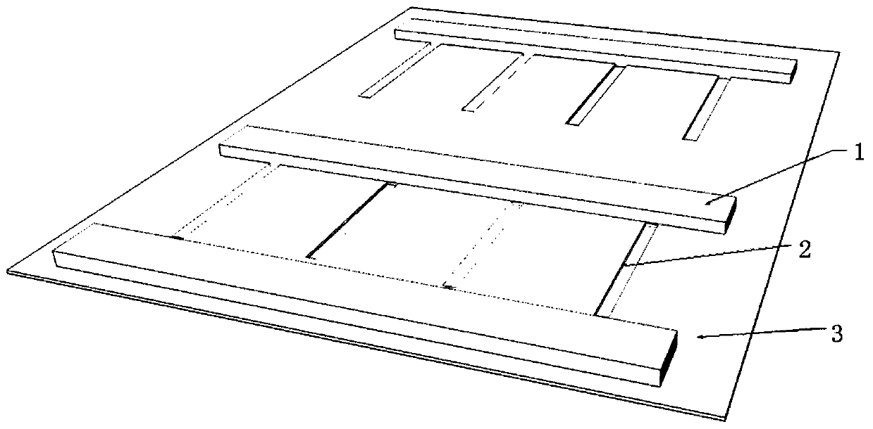
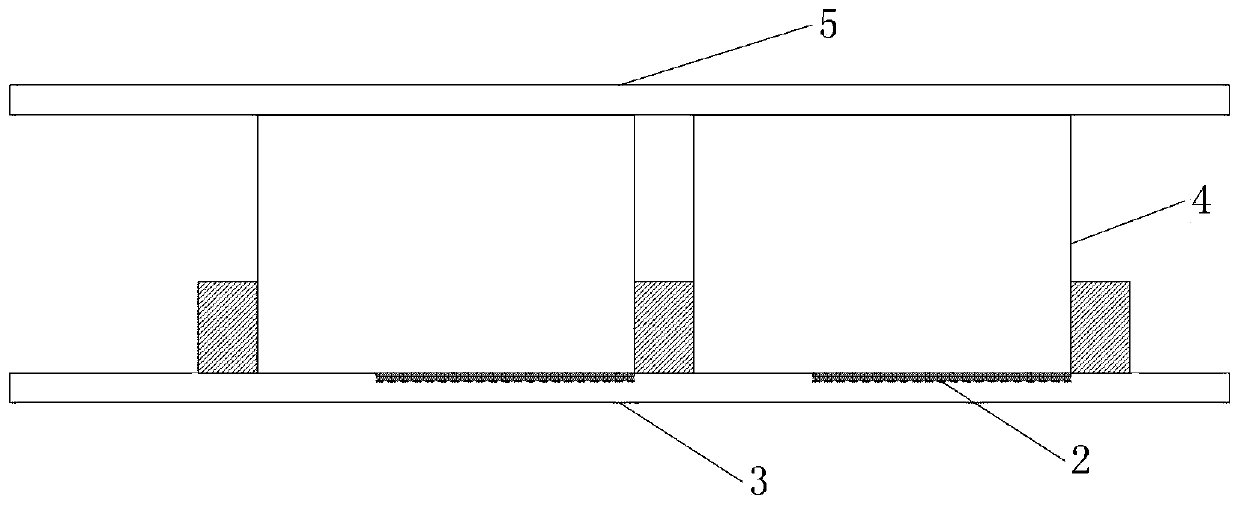
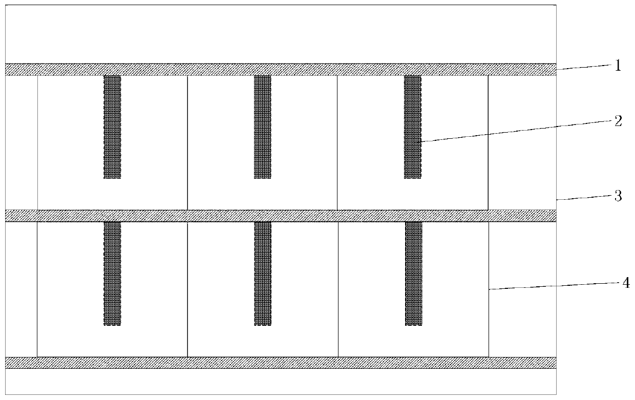
[0025] Such as Figure 1-4 As shown, the design method of the semiconductor chip self-alignment pendulum provided by the present invention, the method includes the following processes:

[0026] Step 101: The semiconductor chip self-alignment swing plate design includes a silicon wafer base, an etching groove, an alignment bar, and a flipping plate.

[0027] Step 102: The etching groove (as shown in the figure) is located on the base of the silicon wafer, and the etching groove is prepared by dry etching and wet etching, and the size of the etching groove is consistent with the chip to be placed The size is consistent (for example, the commonly used high-power semiconductor laser chip size i...


PUM


Abstract

The invention discloses a self-aligning pendulous reed for a semiconductor chip, belongs to the field of the photoelectronic technique, and can be used for the placing and alignment of a semiconductorlight-emitting device chip. An alignment bar is set in the longitudinal direction of the surface of a silicon chip substrate, and the silicon chip substrate is provided with a series of etching slotswhich are the same. The etching slots are arranged in the lateral direction of the surface of the silicon chip substrate. A heat sink is placed on the silicon chip substrate, and an overturning plateis placed on the heat sink. A side edge of the heat sink is aligned with a side edge of a tube core placing in the etching slot. The pendulous reed is simpler in structure, and is lower in design andmanufacturing cost. The pendulous reed is simple, and does not need other redundant devices. The overall size of the pendulous reed is far less than the size of a conventional pendulous reed clampingtool, so the whole pendulous reed can be placed in a nitrogen cover for operation, thereby reducing the oxidation of a cavity surface. Meanwhile, the devices employed by the pendulous reed do not contain metal, so the operation is cleaner.

Description

technical field [0001] The invention relates to a semiconductor chip self-alignment pendulum and a sintering method thereof, which belong to the field of optoelectronic technology and can be applied to placement and alignment of semiconductor light-emitting device chips. Background technique [0002] Semiconductor laser is a new type of optical device with small size, simple structure and low price. Since its appearance, it has triggered technological changes in many fields, and has triggered technological changes in many fields such as optical communication, Internet, information storage, laser processing, and laser display. , formed a new high-tech industrial cluster, and achieved huge economic and social benefits. Since the semiconductor laser has the characteristics of small size and high power, the heat dissipation of the die is a key factor affecting the life and stability of the semiconductor laser. The widely used solution is to sinter the semiconductor laser tube c...

Claims


Application Information

Patent Timeline
Patent Type & Authority Patents(China)
IPC IPC(8): H01S5/022
CPCH01S5/02375
Inventor 崔碧峰孔真真黄欣竹李莎房天啸郝帅
Owner BEIJING UNIV OF TECH
Why Eureka
Try Eureka