Coupling inductance quasi-Z source inverter based on voltage doubling capacitor and modulation method of coupling inductance quasi-z source inverter

A technology of coupled inductance and voltage doubling capacitor, which is applied in the direction of converting irreversible DC power input into AC power output, electrical components, and output power conversion devices, etc., can solve the limitation of boosting capability and increase the harmonic content of output voltage. , large resonant current and other problems, to achieve the effect of suppressing resonant current, improving boost capability and reducing voltage stress

Inactive Publication Date: 2018-02-09
HARBIN INST OF TECH
View PDF5 Cites 0 Cited by
  • Summary
  • Abstract
  • Description
  • Claims
  • Application Information

AI Technical Summary

Problems solved by technology

[0005] The present invention aims to solve the problem that the traditional Z-source inverter’s boosting capability is limited by the cut-through time. If the cut-through time is too large, the harmonic content of the output voltage will increase, and the input current of the DC power supply will be intermittent. Resonant currents, causing problems with device damage

Method used


Image

  • Coupling inductance quasi-Z source inverter based on voltage doubling capacitor and modulation method of coupling inductance quasi-z source inverter
  • Coupling inductance quasi-Z source inverter based on voltage doubling capacitor and modulation method of coupling inductance quasi-z source inverter
  • Coupling inductance quasi-Z source inverter based on voltage doubling capacitor and modulation method of coupling inductance quasi-z source inverter

Examples


specific Embodiment approach 1

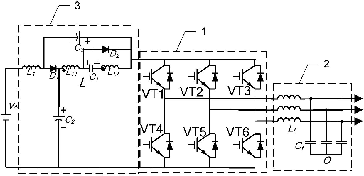
[0035] Specific implementation mode one: refer to figure 1 Specifically illustrate the present embodiment, the coupled inductance quasi-Z source inverter based on the voltage doubler capacitor described in the present embodiment includes a three-phase inverter 1 and an output filter 2,

[0036] The AC signal output terminal of the three-phase inverter 1 is connected to the AC signal input terminal of the output filter 2, and the voltage output by the filtered signal output terminal of the output filter 2 supplies power to the load;

[0037] It is characterized in that it also includes a quasi-Z source network 3,

[0038] The quasi-Z source network 3 includes an electrolytic capacitor C 1 -C 3 , coupled inductance L, inductance L 1 and diode D 1 -D 2 ,

[0039] The positive pole of the DC power supply is connected to the inductance L 1 One end of the inductor L 1 The other end of the diode D is connected simultaneously 1 positive electrode and electrolytic capacitor C ...

specific Embodiment approach 2

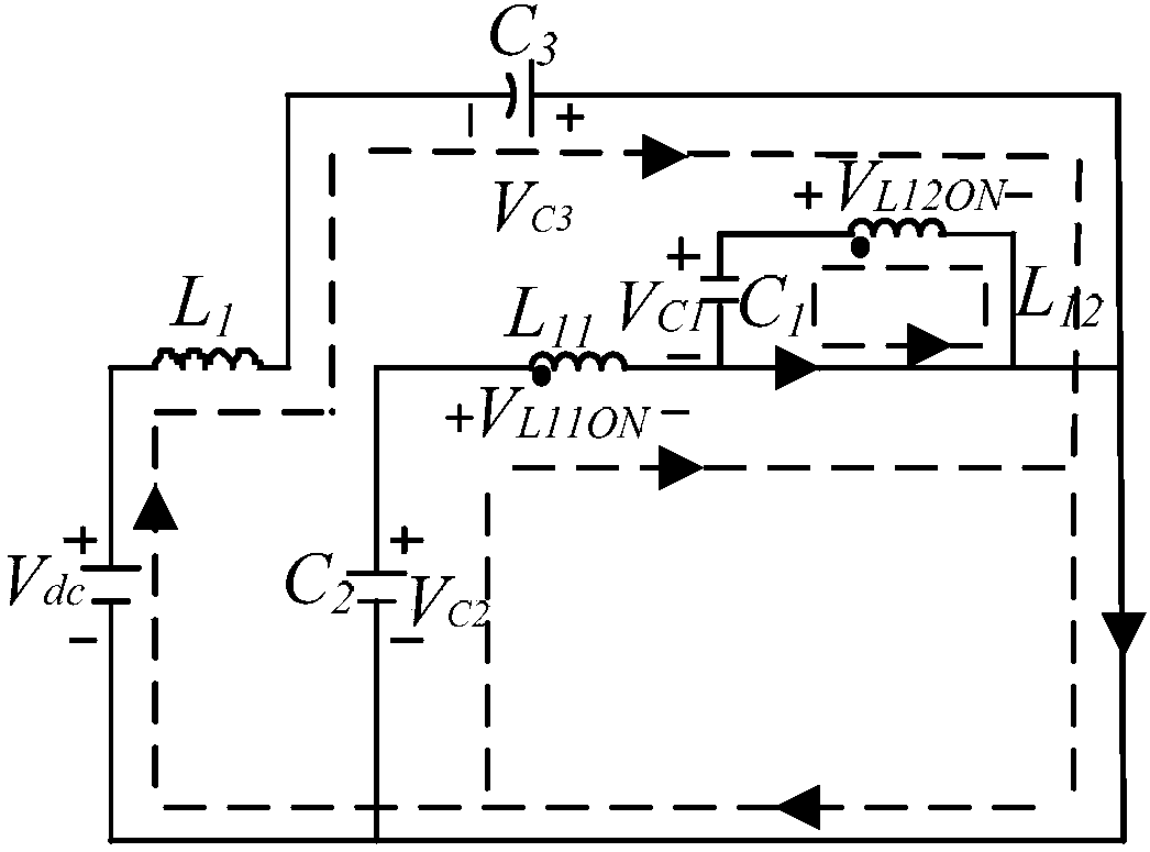
[0043] Specific implementation mode two: refer to Figure 2 to Figure 3 This embodiment is described in detail. This embodiment is to further illustrate the coupled inductance quasi-Z source inverter based on the voltage doubler capacitor described in the first embodiment. In this embodiment, the three-phase inverter 1 has two kinds of work state, which are straight-through state and normal state;

[0044] When the upper and lower bridge arms of the three-phase inverter 1 are in the straight-through state, the quasi-Z source network 3 is disconnected from the three-phase inverter 1, and the electrolytic capacitor C 3 and DC power to the inductor L 1 charging, the electrolytic capacitor C 2 Charge the primary winding of the coupled inductor, the secondary winding L of the coupled inductor L 12 through diode D 2 to the electrolytic capacitor C 1 Charge to achieve double voltage;

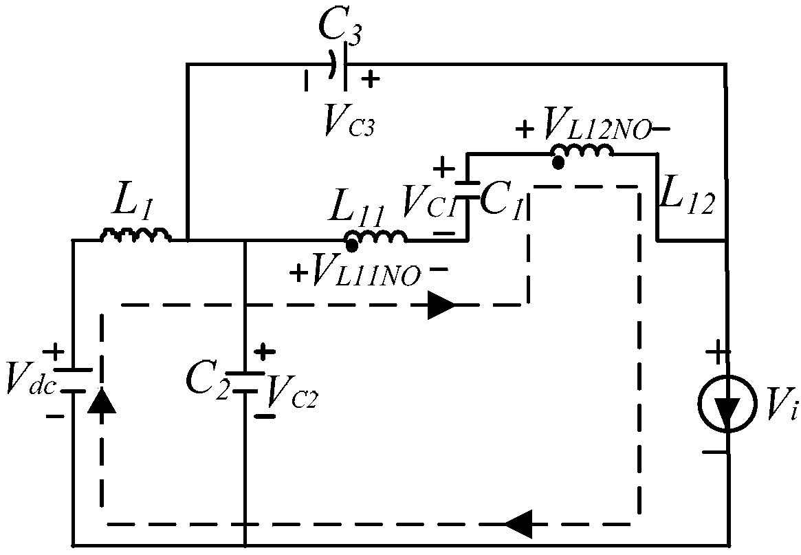
[0045] When the three-phase inverter 1 is in a normal working state, the quasi-Z source netwo...

specific Embodiment approach 3

[0046] Specific embodiment three: This embodiment is to further explain the coupled inductance quasi-Z source inverter based on the voltage doubler capacitor described in the second specific embodiment. In this embodiment, the voltage doubling is realized, specifically:

[0047] Set in a switching cycle T, the duration of the straight-through state is T 0 , then in the straight-through state, the voltage in the quasi-Z source network 3 is:

[0048]

[0049] In the formula, V L1ON Inductance L in the through state 1 Voltage across the terminal, V L11ON is the voltage across the primary winding of the coupled inductor in the through state, V L12ON is the voltage across the secondary winding of the coupled inductor in the straight-through state, V dc is the DC voltage input by the quasi-Z source network, V i is the input terminal voltage of the three-phase inverter, V C1 is the electrolytic capacitor C in the through state 1 voltage, V C2 is the electrolytic capacitor ...


PUM


Abstract

The invention discloses a coupling inductance quasi-z source inverter based on a voltage doubling capacitor and a modulation method of the coupling inductance quasi-z source inverter, and relates to the technical field of inverters. The invention aims at solving the problems that the voltage boosting capability of the traditional Z-source inverter is limited by straight-through time and the outputvoltage harmonic content is increased due to the fact that the straight-through time is too large, the input current of a DC power supply is interrupted, and large resonant current can be generated when a device is started to cause damage to the device. When an upper bridge arm and a lower bridge arm of a three-phase inverter are in a straight-through state, a quasi-z source network is disconnected to the three-phase inverter, an electrolytic capacitor C3 and the DC power supply charge an inductor L1, an electrolytic capacitor C2 charges a primary winding of a coupling inductor, and a secondary winding L12 of the coupling inductor L charges an electrolytic capacitor C1 through a diode D2, so that voltage doubling is realized. The voltage boosting capability of the circuit is improved.

Description

technical field [0001] The invention relates to a coupled inductance quasi-Z source inverter based on a voltage doubling capacitor and a modulation method thereof, and belongs to the technical field of inverters. Background technique [0002] In the energy conversion and transmission process of new energy power generation, the inverter is very important. However, the traditional voltage source and current source inverters cannot realize step-up and step-down control at the same time, so the application occasions are greatly limited. If a DC-DC converter is added to the DC side, the loss and cost will be increased. At the same time, in order to avoid the same For the occurrence of the bridge arm shoot-through phenomenon, it is necessary to add dead time, which will lead to distortion of the output waveform. [0003] In the traditional VSI, the upper and lower switching tubes of the same bridge arm are never allowed to be turned on at the same time, because any bridge arm thr...

Claims


Application Information

Patent Timeline
Patent Type & Authority Applications(China)
IPC IPC(8): H02M7/44H02M7/46
CPCH02M7/44H02M7/46H02M1/0067
Inventor 刘洪臣纪玉亮
Owner HARBIN INST OF TECH
Why Eureka
Try Eureka