Current sampling circuit
A current sampling and voltage sampling technology, applied in electrical components, adjusting electrical variables, converting DC power input to DC power output, etc., can solve the problems of high power consumption, limitation, and temperature rise of current sampling resistors
- Summary
- Abstract
- Description
- Claims
- Application Information
AI Technical Summary
Problems solved by technology
Method used
Image
Examples
no. 1 example
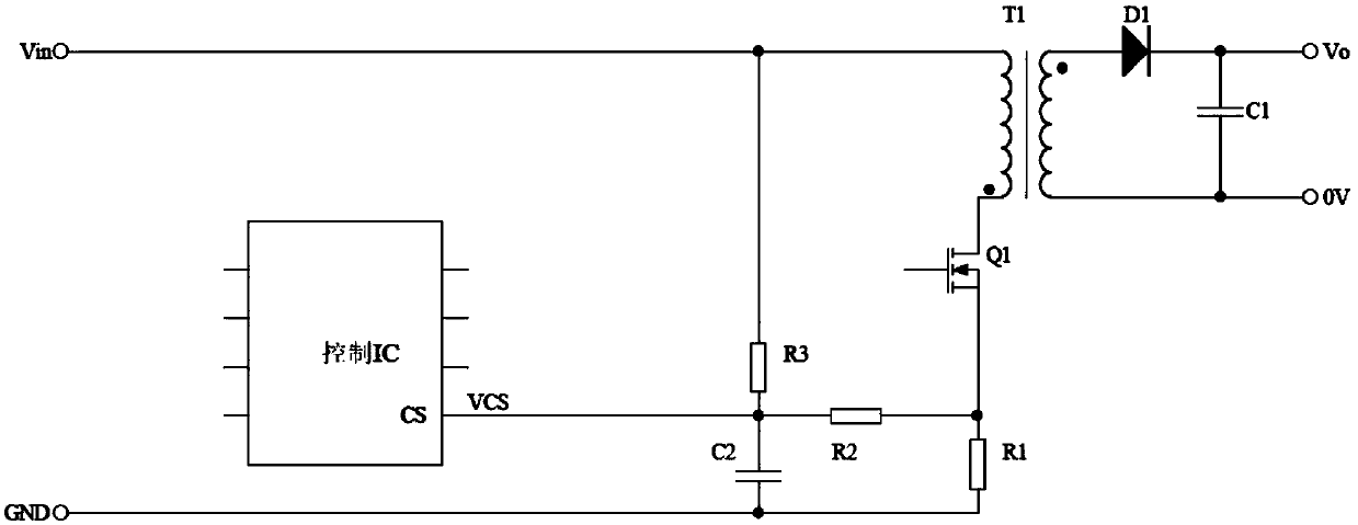
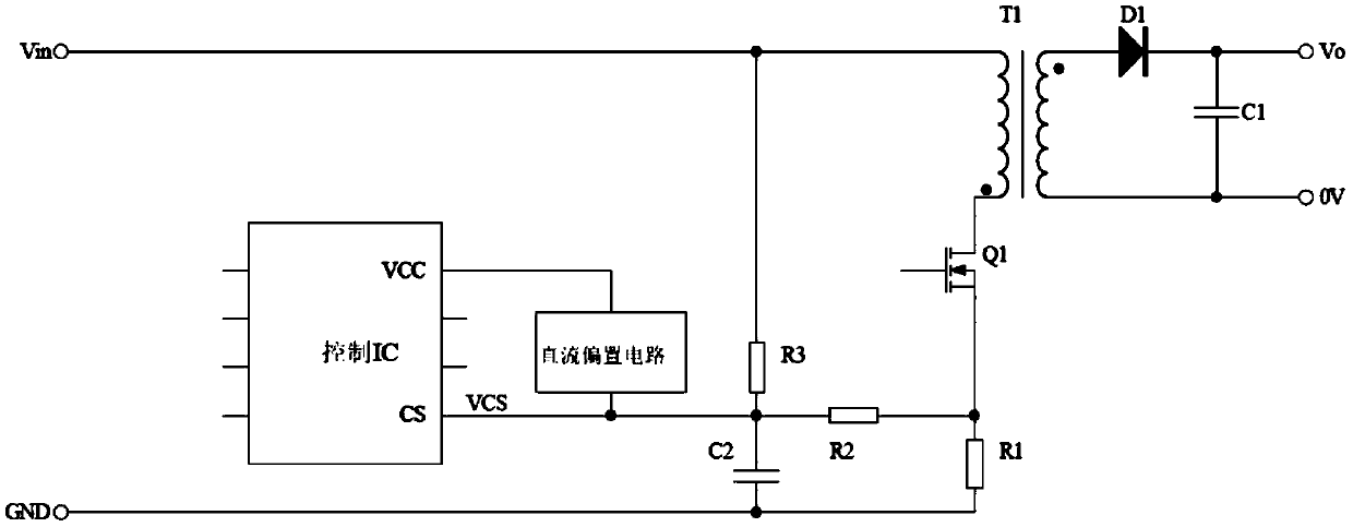
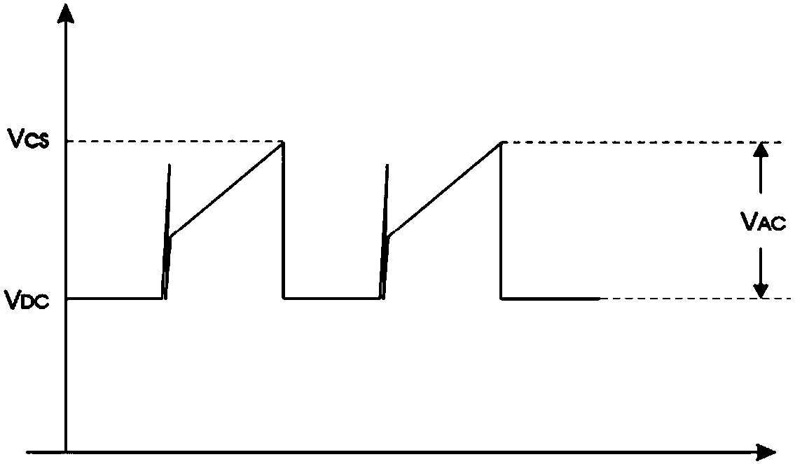
[0024] Figure 4 A schematic diagram of the first embodiment is shown, and its power stage topology is a flyback topology. The flyback topology circuit includes a transformer T1, an N-MOS transistor Q1, a first diode D1, and a first capacitor C1. The transformer includes a first primary winding and a first secondary winding; the flyback circuit The connection relationship is as follows: the opposite end of the first primary winding is connected to the positive pole of the power input, the same end of the first primary winding is connected to the drain of the N-MOS transistor Q1, and the N-MOS The source of the tube Q1 outputs current to the current sampling circuit of the present invention; the terminal with the same name of the first secondary winding is connected to the anode of the first diode D1, and the cathode of the first diode D1 is connected to the output terminal positive pole, the opposite end of the first secondary winding is connected to the negative pole of the ...
no. 2 example
[0029] Figure 5 The schematic diagram of the second embodiment is shown, and its power stage topology is a flyback topology. The difference from the first embodiment is that the DC bias circuit connects the second resistor and the first resistor through a constant current source IC2 The voltage generated above is realized, the anode of the constant current source IC2 is connected to the positive pole of the power input, and the cathode of the constant current source IC2 is connected to the first terminal of the second capacitor C2, that is, the cathode of the constant current source IC2 is connected to the first terminal of the second capacitor C2. Control the current sampling pin of IC.
[0030] The working principle is: the output current of the constant current source flows through R2 and R1. Since the output current of the constant current source is relatively stable, the voltage drop generated on R2 and R1 is also relatively stable, so that the same as the implementation...
no. 3 example
[0032] On the basis of the first embodiment and the second embodiment, a voltage feedforward circuit is added, which is connected between the positive pole of the power input and the current sampling pin CS of the control IC.
[0033] The voltage feedforward circuit of the present invention includes a third resistor R3, the first terminal of R3 is connected to the positive pole of the power input, and the second terminal of R3 is connected to the first terminal of R2.
[0034] When the input voltage is not fixed or the input voltage range is wide, the product overcurrent point can be adjusted through the first resistor, the third resistor combined with the fourth resistor and the second resistor, or by The first resistor and the third resistor are adjusted in combination with the constant current source IC2 and the second resistor, so that the overcurrent point of the product is relatively stable within the input voltage range, and at the same time, it can be compared with the ...
PUM
 Abstract
Description
Claims
Application Information
 - R&D
- Intellectual Property
- Life Sciences
- Materials
- Tech Scout
- Unparalleled Data Quality
- Higher Quality Content
- 60% Fewer Hallucinations
Browse by: Latest US Patents, China's latest patents, Technical Efficacy Thesaurus, Application Domain, Technology Topic, Popular Technical Reports.
© 2025 PatSnap. All rights reserved.Legal|Privacy policy|Modern Slavery Act Transparency Statement|Sitemap|About US| Contact US: help@patsnap.com


