Terahertz near-field radiation enhancement device based on two-dimensional electron concentration modulation

A terahertz near-field, concentration modulation technology, applied in instruments, nonlinear optics, optics, etc., can solve problems such as two-dimensional electron concentration difference, and achieve the effect of simple device and enhanced terahertz near-field radiation intensity

Active Publication Date: 2020-08-04
UNIV OF SHANGHAI FOR SCI & TECH
View PDF7 Cites 0 Cited by
  • Summary
  • Abstract
  • Description
  • Claims
  • Application Information

AI Technical Summary

Problems solved by technology

[0004] The present invention aims at the problem that there are great difficulties in enhancing the intensity of terahertz near-field radiation at present, and proposes a terahertz near-field radiation enhancement device based on two-dimensional electron concentration modulation. Voltage adjustment changes the movement of two-dimensional electrons on the semiconductor material graphene, forming a method of two-dimensional electron concentration difference to generate defect cavities, and stimulating the enhancement of terahertz radiation intensity

Method used


Image

  • Terahertz near-field radiation enhancement device based on two-dimensional electron concentration modulation
  • Terahertz near-field radiation enhancement device based on two-dimensional electron concentration modulation
  • Terahertz near-field radiation enhancement device based on two-dimensional electron concentration modulation

Examples


Embodiment Construction

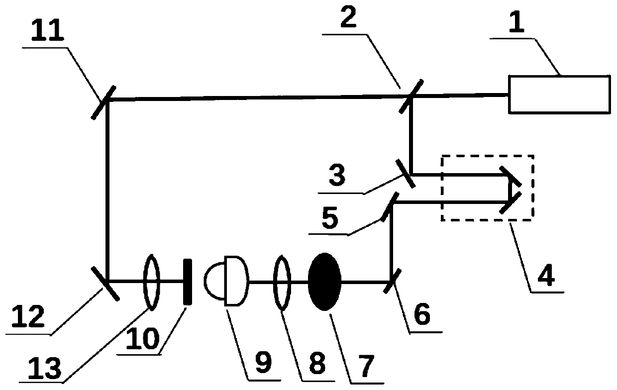
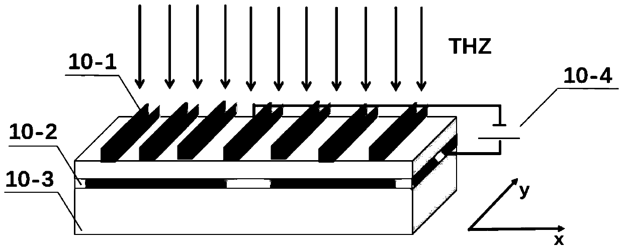
[0013] like figure 1 Shown is a schematic diagram of the structure of a terahertz near-field radiation enhancement device based on two-dimensional electron concentration modulation. The device includes a laser light source 1, a beam splitter 2, a first reflector 3, a mechanical delay line 4, a second reflector 5, and a third reflector mirror 6, chopper 7, first lens 8, photoconductive antenna 9, sub-grating field effect transistor 10 controlled by bias voltage, fourth mirror 11, fifth mirror 12, second lens 13. like figure 2 The schematic diagram of the sub-grating field effect transistor controlled by bias voltage is shown, wherein the sub-grating field effect transistor 10 controlled by bias voltage includes the grating layer 10-1 of the gate, the semiconductor layer 10-2 and the dielectric substrate 10 from top to bottom -3, applying a bias voltage 10-4 between the gate of the grating layer 10-1 and the semiconductor layer 10-2.

[0014] The femtosecond laser output from...


PUM


Abstract

The invention relates to a terahertz near-field radiation enhancement device based on two-dimensional electron concentration modulation. Femtosecond laser outputted from a laser light source is divided into two beams by a beam splitting piece. The beam splitting piece reflects the light beams to serve as pump light, the pump light is focused on a photoconductive antenna to generate terahertz waves, the terahertz waves enter a beam splitting grating field-effect transistor, bias voltage is applied to a grid electrode on a grating layer and a semiconductor layer of the beam splitting grating field-effect transistor, a defect cavity is formed in the semiconductor layer below the metal grid electrode, and terahertz near-field radiation passing the defect cavity can be enhanced. After transmitted light of the beam splitting piece is focused, the transmitted light serving as terahertz wave probe light is transmitted to a dielectric medium substrate on the other side of the beam splitting grating field-effect transistor, and the terahertz waves enhanced by the near-field radiation are detected. Terahertz near-field radiation intensity can be enhanced only by changing the bias voltage andadjusting concentration difference, and the device is easily set up, simple and convenient to operate and applicable to development of advanced technologies such as terahertz imaging technologies related to the terahertz near-field radiation intensity.

Description

technical field [0001] The invention relates to a terahertz near-field radiation enhancement technology, in particular to a terahertz near-field radiation enhancement device based on two-dimensional electron concentration modulation. Background technique [0002] In recent decades, terahertz waves have become an important research topic in the field of physics in the world due to its wide application prospects. Terahertz waves refer to electromagnetic waves (1THz=10 12 Hz), which lies between microwaves and infrared waves in the electromagnetic spectrum. The special electromagnetic spectrum position of terahertz wave makes it have many unique advantages: it has the characteristics of rich information, high space-time coherence, low photon energy, etc., and has great application value in scientific fields such as astronomy, biology, computer, and communication. At present, the main applied research includes terahertz time-domain spectroscopy technology, terahertz imaging te...

Claims


Application Information

Patent Timeline
Patent Type & Authority Patents(China)
IPC IPC(8): G02F1/015
CPCG02F1/015G02F2203/13
Inventor 刘志佳彭滟朱亦鸣孙召召寇天一肖海成唐心雨刘可盈庄松林
Owner UNIV OF SHANGHAI FOR SCI & TECH
Why Eureka
Try Eureka