Array substrate, preparation method, display panel and display device

A technology for array substrates and display panels, which is applied in the fields of preparation methods, array substrates, display panels, and display devices, and can solve problems such as uneven lighting brightness of electroluminescent devices and decreased material utilization

Inactive Publication Date: 2018-02-23
BOE TECH GRP CO LTD
View PDF3 Cites 11 Cited by
  • Summary
  • Abstract
  • Description
  • Claims
  • Application Information

AI Technical Summary

Problems solved by technology

[0004] The invention provides an array substrate, a preparation method, a display panel and a display device to solve the problems of uneven lighting brightness of electroluminescent devices and greatly reduced material utilization rate existing in existing solutions

Method used


Image

  • Array substrate, preparation method, display panel and display device
  • Array substrate, preparation method, display panel and display device
  • Array substrate, preparation method, display panel and display device

Examples


Embodiment 1

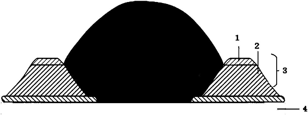
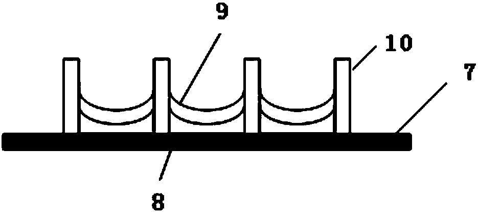
[0035] refer to image 3 , shows a schematic structural view of an array substrate provided by an embodiment of the present invention. As shown in the figure, the array substrate may include a substrate 7 and an array of anode layers 8 arranged on the substrate 7, wherein, at a distance from each anode layer 8 Within the preset distance range from the edge, the thickness of each anode layer 8 gradually increases along the direction from the center to the edge of each anode layer 8 .

[0036] In the prior art solution, the wet film forming process needs to remove excess solvent through a subsequent process, so as to dry and form the required film. In the drying process, when the ink drop falls into the substrate or pixel, due to the shape of the ink drop, the evaporation rate of the central part with a smaller volume / unit area ratio and the edge part with a larger volume / unit area ratio in the ink droplet different, so the ink dries faster at the edges. With the continuous vo...

Embodiment 2

[0053] refer to Figure 5 , which shows a flow chart of the steps of a method for preparing a substrate provided in an embodiment of the present invention, which may include the following steps:

[0054] Step 101: providing a substrate.

[0055] In the embodiment of the present invention, before the preparation of the anode layer is completed, a substrate needs to be provided first, and the substrate may be, but not limited to, an insulating substrate such as a glass substrate or a plastic substrate.

[0056] The substrate includes a substrate, and the preparation method of the substrate mainly includes: sequentially forming a gate layer, a gate insulating layer, a semiconductor layer, a source and drain layer, a passivation layer and a flat layer on the substrate.

[0057] The method for preparing the substrate provided in the embodiment of the present invention is an improvement on the process of the anode layer. The method for preparing the substrate is the same as that co...


PUM


Abstract

The invention provides an array substrate, a preparation method, a display panel and a display device. The array substrate comprises a substrate and positive electrode layers arranged on the substratein an array, wherein the thickness of each positive electrode layer is gradually increased in the direction from the center of each positive electrode layer to the edge of each positive electrode layer in a preset distance range to the edge of each positive electrode layer. The positive electrode layers arranged on the substrate in the array are such manufactured that the thickness of each positive electrode layer is gradually increased in the direction from the center of each positive electrode layer to the edge of each positive electrode layer in the preset distance range to the edge of each positive electrode layer, and then a coffee-ring effect can be effectively avoided when a luminescent material is continuously printed on an electrode, so that a film with uniform thickness is formed, the uniformity of the printed film is improved, the flatness of the pixel film is guaranteed, the brightness for electroluminescence device illumination can be uniform, and the utilization efficiency of the material is further improved.

Description

technical field [0001] The invention relates to the display field, in particular to an array substrate, a preparation method, a display panel and a display device. Background technique [0002] In the field of electroluminescent devices (OLED or QLED) and liquid crystal (LCD) displays, wet film-forming processes such as inkjet printing are usually used to form organic functional layer films and color filter structures. A necessary step of these wet film-forming processes is that excess solvent needs to be removed through subsequent processes, so as to dry and form the desired film. And this drying process to remove the solvent determines the morphology of the formed film. For optoelectronic display devices, the poor morphology and uniformity of the dry film have a great impact on the life of the device and the display effect. [0003] In the drying process, when the ink drop falls into the substrate or pixel, due to the shape of the ink drop, the evaporation rate of the ce...

Claims


Application Information

Patent Timeline
Patent Type & Authority Applications(China)
IPC IPC(8): H01L27/32H01L51/52H01L51/56
CPCH10K59/122H10K50/813H10K71/00H10K71/60H10K2102/351H10K59/131H10K50/81
Inventor 孙凌红
Owner BOE TECH GRP CO LTD
Why Eureka
Try Eureka