Surface enhanced Raman substrate and preparation method thereof

A surface-enhanced Raman and substrate technology, applied in Raman scattering, measuring devices, instruments, etc., can solve the problems of poor reproducibility of Raman scattering signals, and achieve the effect of regular arrangement, good reproducibility and uniform size

Inactive Publication Date: 2018-03-02
LANZHOU UNIVERSITY
View PDF1 Cites 7 Cited by
  • Summary
  • Abstract
  • Description
  • Claims
  • Application Information

AI Technical Summary

Problems solved by technology

[0007] The present invention provides a surface-enhanced Raman substrate and its preparation method, which aims to at least partially solve the existing technical problem of poor reproducibility of Raman scattering signals excited by the substrate

Method used


Image

  • Surface enhanced Raman substrate and preparation method thereof
  • Surface enhanced Raman substrate and preparation method thereof
  • Surface enhanced Raman substrate and preparation method thereof

Examples


no. 1 example

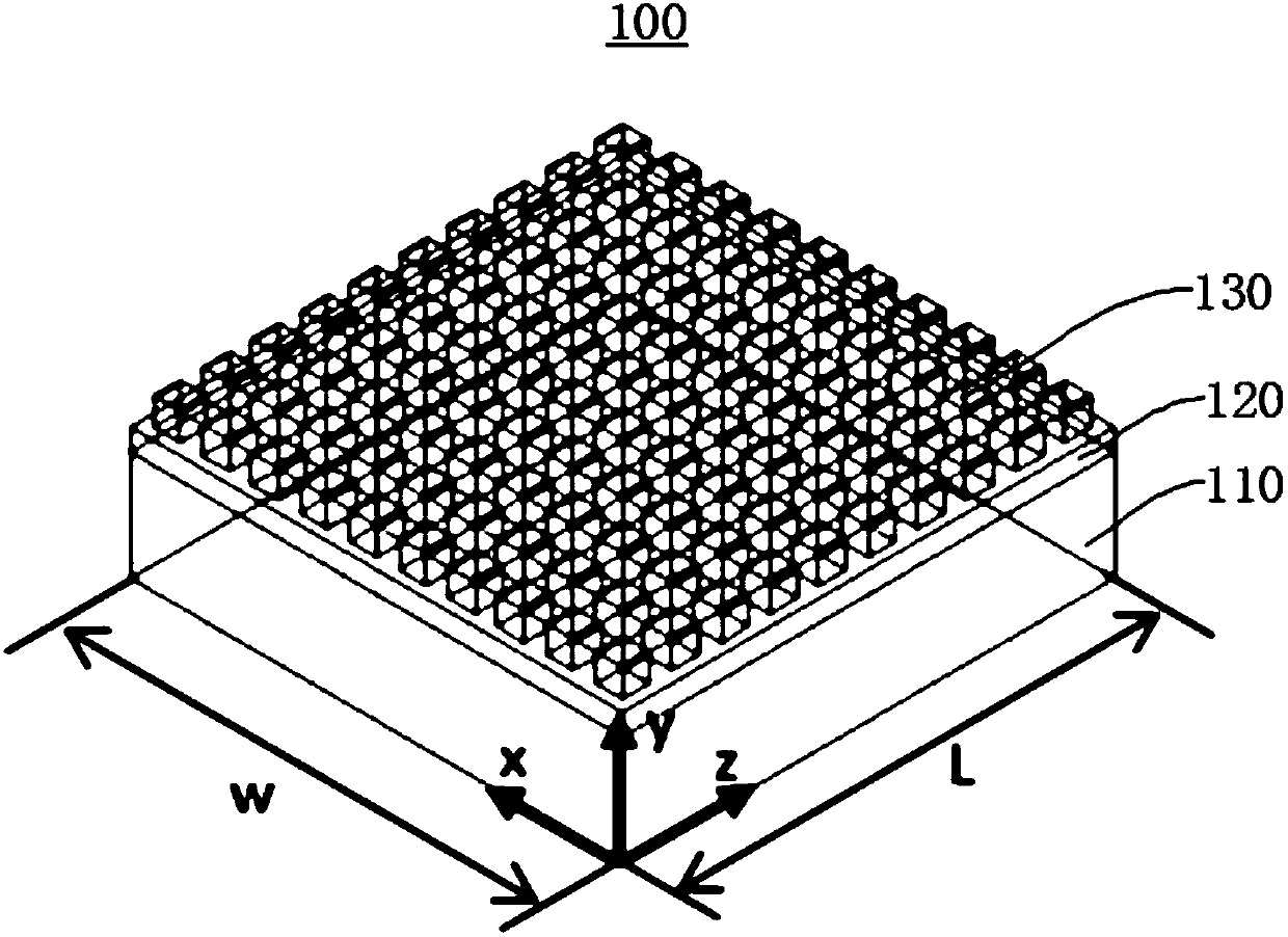
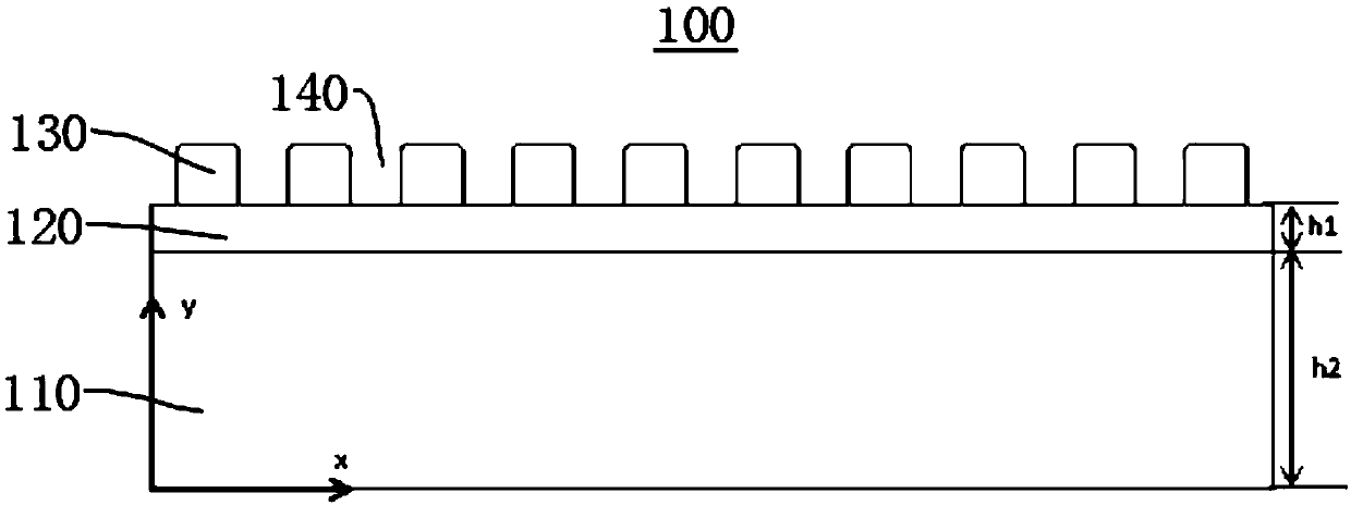
[0042] see figure 1 and figure 2, this embodiment provides a surface-enhanced Raman substrate 100, the surface-enhanced Raman substrate 100 is used to detect liquid samples, and the surface-enhanced Raman substrate 100 includes a substrate 110, a gold film 120 and gold nanocubes 130.

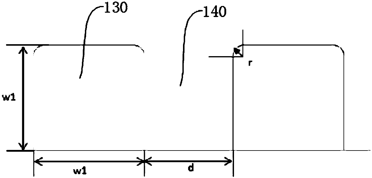
[0043] The substrate 110 is formed of silicon material, and the gold film 120 is disposed on the substrate 110 . Before forming the gold film 120 on the substrate 110 , a titanium layer is first formed on the substrate 110 , and then the gold film 120 is formed on the titanium layer. The gold nanocubes 130 are arranged on the gold film 120, and the gold nanocubes 130 are arranged in a matrix, and there are gaps 140 between the gold nanocubes 130, and the gaps 140 are used to inject liquid samples to be tested.

[0044] The substrate 110 has a cuboid structure, the length L of the substrate 110 is 2000 nm, the width W of the substrate 110 is 2000 nm, and the height h2 of the substrate 110 is 11...

no. 2 example

[0056] This embodiment provides a method for preparing a surface-enhanced Raman substrate, the method comprising:

[0057] S1: A silicon material is used to form a substrate.

[0058] The substrate 110 has a cuboid structure, the length L of the substrate 110 is 2000 nm, the width W of the substrate 110 is 2000 nm, and the height h2 of the substrate 110 is 110 nm.

[0059] S2: Depositing a titanium layer on the surface of the substrate, and plating a gold film on the titanium layer.

[0060] The gold film is formed by vacuum evaporation. The length of the gold film 120 is 2000 nm, the width of the gold film 120 is 2000 nm, and the gold film 120 completely covers the upper surface of the substrate 110 . The thickness of the gold film 120 is h1+W1=90nm.

[0061] S3: forming matrix-arranged gold nanocubes on the surface of the gold film by a metal lift-off method, with gaps between the gold nanocubes, and the gaps are used to inject liquid samples to be tested.

[0062] The s...


PUM

PropertyMeasurementUnit
lengthaaaaaaaaaa
widthaaaaaaaaaa
radiusaaaaaaaaaa

Abstract

The invention provides a surface enhanced Raman substrate and a preparation method thereof and relates to the technical field of material structure detection. The surface enhanced Raman substrate is used for detecting a liquid sample; the surface enhanced Raman substrate comprises a substrate, a gold film and gold nano-cubes; the substrate is made of a silicon material; the gold film is arranged on the substrate and the gold nano-cubes are arranged on the gold film; the gold nano-cubes are arrayed in a matrix; gaps are formed between the gold nano-cubes; the gaps are used for injecting the liquid sample to be detected. The gold nano-cubes are arrayed in the matrix and the formed gaps are regularly arrayed and have a uniform size; after the product to be detected is injected to the gaps, the product to be detected has good uniformity and an excited solution Raman scattering signal is enhanced; the surface enhanced Raman substrate has high sensitivity and good repeatability and structureinformation of a molecular level of the product to be detected can be relatively accurately and clearly detected.

Description

technical field [0001] The invention relates to the technical field of material structure detection, in particular to a surface-enhanced Raman substrate and a preparation method thereof. Background technique [0002] Surface-Enhanced Raman Scattering (SERS) refers to a phenomenon in which the surface of a rough noble metal enhances the Raman scattering signal emitted by the molecules of substances adsorbed on the surface under the excitation of incident light. [0003] The enhancement of the Raman scattering signal of the molecule comes from the oscillation of the surface electrons generated by the rough surface under the illumination. When the frequency of the incident light matches the frequency of the plasma of the metal itself, the electron oscillation reaches the maximum, thus generating a phenomenon similar to that on the metal surface. An additional local electromagnetic field with the same frequency as the incident light, and the additional local electromagnetic fiel...

Claims


Application Information

Patent Timeline
Patent Type & Authority Applications(China)
IPC IPC(8): G01N21/65
CPCG01N21/658
Inventor 李月娥蔡可苏王忠
Owner LANZHOU UNIVERSITY
Why Eureka
Try Eureka