Semiconductor die package and method of producing the package

A semiconductor tube and die technology, applied in the fields of semiconductor devices, semiconductor/solid-state device manufacturing, semiconductor/solid-state device components, etc., can solve the problems of not allowing independent packaging and simple testing of logic dies, and reduce the overall package size. and the effect of interconnect length, cost reduction

Active Publication Date: 2018-03-09
INTERUNIVERSITAIR MICRO ELECTRONICS CENT (IMEC VZW)
View PDF3 Cites 7 Cited by
  • Summary
  • Abstract
  • Description
  • Claims
  • Application Information

AI Technical Summary

Problems solved by technology

However, these solutions do not allow for independent packaging and simple testing of the logic die

Method used


Image

  • Semiconductor die package and method of producing the package
  • Semiconductor die package and method of producing the package
  • Semiconductor die package and method of producing the package

Examples


Embodiment Construction

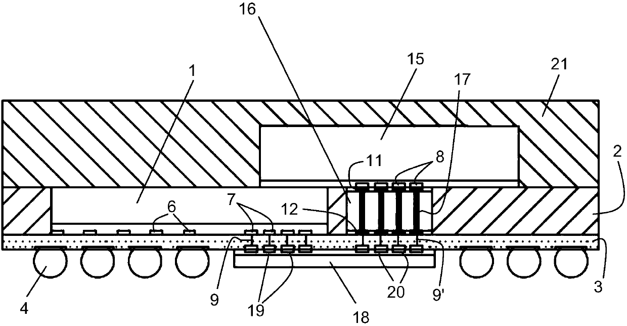
[0033] figure 1 The package shown includes logic die 1 and memory die 15 with interconnected I / O contact arrays 7 / 8. For example, memory die 15 may be a DRAM die configured according to a wide I / O standard. Both contact arrays 7 and 8 are in this case configured according to this standard, ie each array comprises 4 groups of 6x73 contact pads with a pitch of 40 μm. However, the invention is not limited to such devices, and figure 1The embodiments are to be understood as merely exemplifying typical fields of application of the invention. The logic die 1 is embedded in a substrate 2 formed of a mold material and comprises a redistribution layer (RDL) 3 on the front side of the substrate. Package-level solder balls 4 are mounted on contact pads 5 provided on the surface of the RDL 3 for establishing connections to the front side of the logic die 1 by circuitry (not shown) contained in the RDL 3. on the contact terminal 6 provided on the connection. The front side of the logi...


PUM


Abstract

A package including a first die embedded in a reconstructed wafer obtainable by the known FO-WLP or eWLB technologies is disclosed. In one aspect and in addition to the first die, a Through SubstrateVia insert is embedded in the wafer, the TSV insert being a separate element, possibly a silicon die with metal filled vias interconnecting contacts on the front and back sides of the insert. A seconddie is mounted on the back side of the substrate, with contacts on the second die in electrical connection with the TSV insert's contacts on the back side of the substrate. On the front side of the substrate, a lateral connecting device is mounted which interconnects the TSV insert's contacts on the front side of the substrate to contacts on the front side of the first die. The lateral connectingdevice and the TSV insert thereby effectively interconnect the contacts on the first and second dies. In another aspect, the lateral connecting device is mounted on a redistribution layer on the front side of the substrate, as it is known from FO-WLP technology.

Description

technical field [0001] The present invention relates to semiconductor processing, and more particularly to the integration of multiple integrated circuit dies in 3D interconnected packages. Background technique [0002] The 3D integration of integrated circuit devices (also known as semiconductor chips or dies) has undergone many developments in recent years. In particular, the integration of two or more dies with a large number of die-to-die interconnects has become challenging in terms of package size and thermal issues. The traditional PoP (Package-on-Package) approach involves packaging two dies (such as an application processor and a memory chip in mobile applications) in separate ball grid array-type packages, and assembling one package on top of the other. The resulting package heights can be problematic, and the package level solder balls do not allow a large number of interconnections to be achieved at the small pitches required for integration, eg, according to w...

Claims


Application Information

Patent Timeline
Patent Type & Authority Applications(China)
IPC IPC(8): H01L25/18H01L23/498H01L23/31H01L21/60
CPCH01L23/3128H01L23/49827H01L24/81H01L25/18H01L2224/81H01L2224/0233H01L2224/02381H01L2224/83005H01L2224/92124H01L23/3135H01L21/561H01L21/568H01L23/5389H01L24/19H01L24/20H01L24/96H01L24/97H01L2224/04105H01L2224/12105H01L2224/16227H01L2224/16235H01L2224/32145H01L2224/32225H01L2224/73203H01L2224/73204H01L2224/73209H01L2224/73253H01L2224/73267H01L2224/81005H01L2224/81815H01L2224/97H01L2924/1431H01L2924/1434H01L2924/1436H01L2924/15192H01L2924/15311H01L25/0652H01L25/50H01L23/147H01L23/5383H01L23/5385H01L2224/08235H01L2224/08145H01L2224/80006H01L2224/83H01L2224/16225H01L2924/00H01L23/538H10B99/00H01L23/481H03K3/36
Inventor E·贝内
Owner INTERUNIVERSITAIR MICRO ELECTRONICS CENT (IMEC VZW)
Why Eureka
Try Eureka